Zuzanna Molenda, Sylvain Chambon, Dario M. Bassani, Lionel Hirsch
{"title":"过氧化物太阳能电池中的电子掺杂","authors":"Zuzanna Molenda, Sylvain Chambon, Dario M. Bassani, Lionel Hirsch","doi":"10.1002/aelm.202400090","DOIUrl":null,"url":null,"abstract":"<p>The popularity of metal halide perovskites is in part the result of their versatility in numerous applications. To date, perovskites are used in their intrinsic, undoped form, as the doping of these materials is not yet adequately mastered. Herein, the recently reported electronic doping of CH<sub>3</sub>NH<sub>3</sub>PbI<sub>3</sub> is employed to fabricate perovskite solar cells in which the interfacial electron transport layer (ETL) is replaced by n-doping of one side of the perovskite film. The doping involves the incorporation of metastable Sm<sup>2+</sup> ions that undergo an in situ oxidation to Sm<sup>3+</sup>, releasing electrons to the conduction band to render the perovskite n-type. In spite of the lack of an ETL, these solar cells have the same efficiency as the samples with the ETL. The open circuit voltage of the doped solar cells increases proportionally to the doping concentration due to the narrowing of the depletion layer thickness at the interface of the perovskite and the top electrode, reaching the value of ≈1 V for the doped ETL-free device, the same as for the reference sample. These proof-of-concept results represent the first step toward perovskite-based devices incorporating a p-n homojunction.</p>","PeriodicalId":110,"journal":{"name":"Advanced Electronic Materials","volume":"10 10","pages":""},"PeriodicalIF":5.3000,"publicationDate":"2024-05-26","publicationTypes":"Journal Article","fieldsOfStudy":null,"isOpenAccess":false,"openAccessPdf":"https://onlinelibrary.wiley.com/doi/epdf/10.1002/aelm.202400090","citationCount":"0","resultStr":"{\"title\":\"Electronic Doping in Perovskite Solar Cells\",\"authors\":\"Zuzanna Molenda, Sylvain Chambon, Dario M. Bassani, Lionel Hirsch\",\"doi\":\"10.1002/aelm.202400090\",\"DOIUrl\":null,\"url\":null,\"abstract\":\"<p>The popularity of metal halide perovskites is in part the result of their versatility in numerous applications. To date, perovskites are used in their intrinsic, undoped form, as the doping of these materials is not yet adequately mastered. Herein, the recently reported electronic doping of CH<sub>3</sub>NH<sub>3</sub>PbI<sub>3</sub> is employed to fabricate perovskite solar cells in which the interfacial electron transport layer (ETL) is replaced by n-doping of one side of the perovskite film. The doping involves the incorporation of metastable Sm<sup>2+</sup> ions that undergo an in situ oxidation to Sm<sup>3+</sup>, releasing electrons to the conduction band to render the perovskite n-type. In spite of the lack of an ETL, these solar cells have the same efficiency as the samples with the ETL. The open circuit voltage of the doped solar cells increases proportionally to the doping concentration due to the narrowing of the depletion layer thickness at the interface of the perovskite and the top electrode, reaching the value of ≈1 V for the doped ETL-free device, the same as for the reference sample. These proof-of-concept results represent the first step toward perovskite-based devices incorporating a p-n homojunction.</p>\",\"PeriodicalId\":110,\"journal\":{\"name\":\"Advanced Electronic Materials\",\"volume\":\"10 10\",\"pages\":\"\"},\"PeriodicalIF\":5.3000,\"publicationDate\":\"2024-05-26\",\"publicationTypes\":\"Journal Article\",\"fieldsOfStudy\":null,\"isOpenAccess\":false,\"openAccessPdf\":\"https://onlinelibrary.wiley.com/doi/epdf/10.1002/aelm.202400090\",\"citationCount\":\"0\",\"resultStr\":null,\"platform\":\"Semanticscholar\",\"paperid\":null,\"PeriodicalName\":\"Advanced Electronic Materials\",\"FirstCategoryId\":\"88\",\"ListUrlMain\":\"https://advanced.onlinelibrary.wiley.com/doi/10.1002/aelm.202400090\",\"RegionNum\":2,\"RegionCategory\":\"材料科学\",\"ArticlePicture\":[],\"TitleCN\":null,\"AbstractTextCN\":null,\"PMCID\":null,\"EPubDate\":\"\",\"PubModel\":\"\",\"JCR\":\"Q2\",\"JCRName\":\"MATERIALS SCIENCE, MULTIDISCIPLINARY\",\"Score\":null,\"Total\":0}","platform":"Semanticscholar","paperid":null,"PeriodicalName":"Advanced Electronic Materials","FirstCategoryId":"88","ListUrlMain":"https://advanced.onlinelibrary.wiley.com/doi/10.1002/aelm.202400090","RegionNum":2,"RegionCategory":"材料科学","ArticlePicture":[],"TitleCN":null,"AbstractTextCN":null,"PMCID":null,"EPubDate":"","PubModel":"","JCR":"Q2","JCRName":"MATERIALS SCIENCE, MULTIDISCIPLINARY","Score":null,"Total":0}
引用次数: 0
摘要
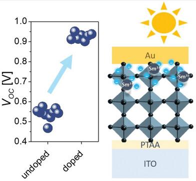
金属卤化物类包晶石之所以广受欢迎,部分原因在于其在众多应用领域的多样性。迄今为止,由于尚未充分掌握这些材料的掺杂技术,因此均以其固有的、未掺杂的形式使用。在本文中,最近报道的 CH3NH3PbI3 电子掺杂被用于制造过氧化物太阳能电池,在这种电池中,过氧化物薄膜的一侧通过 n 掺杂取代了界面电子传输层 (ETL)。这种掺杂涉及掺入可蜕变的 Sm2+ 离子,这些离子在原位氧化成 Sm3+,将电子释放到导带,从而使包晶石成为 n 型。尽管没有 ETL,但这些太阳能电池的效率与带有 ETL 的样品相同。掺杂太阳能电池的开路电压随着掺杂浓度的增加而成正比增加,这是由于包晶和顶部电极界面上的耗尽层厚度变窄所致,无掺杂 ETL 器件的开路电压值≈1 V,与参考样品相同。这些概念验证结果标志着向基于包晶石的 p-n 同结器件迈出了第一步。
The popularity of metal halide perovskites is in part the result of their versatility in numerous applications. To date, perovskites are used in their intrinsic, undoped form, as the doping of these materials is not yet adequately mastered. Herein, the recently reported electronic doping of CH3NH3PbI3 is employed to fabricate perovskite solar cells in which the interfacial electron transport layer (ETL) is replaced by n-doping of one side of the perovskite film. The doping involves the incorporation of metastable Sm2+ ions that undergo an in situ oxidation to Sm3+, releasing electrons to the conduction band to render the perovskite n-type. In spite of the lack of an ETL, these solar cells have the same efficiency as the samples with the ETL. The open circuit voltage of the doped solar cells increases proportionally to the doping concentration due to the narrowing of the depletion layer thickness at the interface of the perovskite and the top electrode, reaching the value of ≈1 V for the doped ETL-free device, the same as for the reference sample. These proof-of-concept results represent the first step toward perovskite-based devices incorporating a p-n homojunction.
期刊介绍:
Advanced Electronic Materials is an interdisciplinary forum for peer-reviewed, high-quality, high-impact research in the fields of materials science, physics, and engineering of electronic and magnetic materials. It includes research on physics and physical properties of electronic and magnetic materials, spintronics, electronics, device physics and engineering, micro- and nano-electromechanical systems, and organic electronics, in addition to fundamental research.


 分享
分享
 求助内容:
求助内容: 应助结果提醒方式:
 扫码关注我们
