{"title":"基于碳纳米管的张量处理单元","authors":"Jia Si, Panpan Zhang, Chenyi Zhao, Dongyi Lin, Lin Xu, Haitao Xu, Lijun Liu, Jianhua Jiang, Lian-Mao Peng, Zhiyong Zhang","doi":"10.1038/s41928-024-01211-2","DOIUrl":null,"url":null,"abstract":"The growth of data-intensive computing tasks requires processing units with higher performance and energy efficiency, but these requirements are increasingly difficult to achieve with conventional semiconductor technology. One potential solution is to combine developments in devices with innovations in system architecture. Here we report a tensor processing unit (TPU) that is based on 3,000 carbon nanotube field-effect transistors and can perform energy-efficient convolution operations and matrix multiplication. The TPU is constructed with a systolic array architecture that allows parallel 2 bit integer multiply–accumulate operations. A five-layer convolutional neural network based on the TPU can perform MNIST image recognition with an accuracy of up to 88% for a power consumption of 295 µW. We use an optimized nanotube fabrication process that offers a semiconductor purity of 99.9999% and ultraclean surfaces, leading to transistors with high on-current densities and uniformity. Using system-level simulations, we estimate that an 8 bit TPU made with nanotube transistors at a 180 nm technology node could reach a main frequency of 850 MHz and an energy efficiency of 1 tera-operations per second per watt. Carbon nanotube networks made with high purity and ultraclean interfaces can be used to make a tensor processing unit that contains 3,000 transistors in a systolic array architecture to improve energy efficiency in accelerating neural network tasks.","PeriodicalId":19064,"journal":{"name":"Nature Electronics","volume":"7 8","pages":"684-693"},"PeriodicalIF":42.3000,"publicationDate":"2024-07-22","publicationTypes":"Journal Article","fieldsOfStudy":null,"isOpenAccess":false,"openAccessPdf":"","citationCount":"0","resultStr":"{\"title\":\"A carbon-nanotube-based tensor processing unit\",\"authors\":\"Jia Si, Panpan Zhang, Chenyi Zhao, Dongyi Lin, Lin Xu, Haitao Xu, Lijun Liu, Jianhua Jiang, Lian-Mao Peng, Zhiyong Zhang\",\"doi\":\"10.1038/s41928-024-01211-2\",\"DOIUrl\":null,\"url\":null,\"abstract\":\"The growth of data-intensive computing tasks requires processing units with higher performance and energy efficiency, but these requirements are increasingly difficult to achieve with conventional semiconductor technology. One potential solution is to combine developments in devices with innovations in system architecture. Here we report a tensor processing unit (TPU) that is based on 3,000 carbon nanotube field-effect transistors and can perform energy-efficient convolution operations and matrix multiplication. The TPU is constructed with a systolic array architecture that allows parallel 2 bit integer multiply–accumulate operations. A five-layer convolutional neural network based on the TPU can perform MNIST image recognition with an accuracy of up to 88% for a power consumption of 295 µW. We use an optimized nanotube fabrication process that offers a semiconductor purity of 99.9999% and ultraclean surfaces, leading to transistors with high on-current densities and uniformity. Using system-level simulations, we estimate that an 8 bit TPU made with nanotube transistors at a 180 nm technology node could reach a main frequency of 850 MHz and an energy efficiency of 1 tera-operations per second per watt. Carbon nanotube networks made with high purity and ultraclean interfaces can be used to make a tensor processing unit that contains 3,000 transistors in a systolic array architecture to improve energy efficiency in accelerating neural network tasks.\",\"PeriodicalId\":19064,\"journal\":{\"name\":\"Nature Electronics\",\"volume\":\"7 8\",\"pages\":\"684-693\"},\"PeriodicalIF\":42.3000,\"publicationDate\":\"2024-07-22\",\"publicationTypes\":\"Journal Article\",\"fieldsOfStudy\":null,\"isOpenAccess\":false,\"openAccessPdf\":\"\",\"citationCount\":\"0\",\"resultStr\":null,\"platform\":\"Semanticscholar\",\"paperid\":null,\"PeriodicalName\":\"Nature Electronics\",\"FirstCategoryId\":\"5\",\"ListUrlMain\":\"https://www.nature.com/articles/s41928-024-01211-2\",\"RegionNum\":1,\"RegionCategory\":\"工程技术\",\"ArticlePicture\":[],\"TitleCN\":null,\"AbstractTextCN\":null,\"PMCID\":null,\"EPubDate\":\"\",\"PubModel\":\"\",\"JCR\":\"Q1\",\"JCRName\":\"ENGINEERING, ELECTRICAL & ELECTRONIC\",\"Score\":null,\"Total\":0}","platform":"Semanticscholar","paperid":null,"PeriodicalName":"Nature Electronics","FirstCategoryId":"5","ListUrlMain":"https://www.nature.com/articles/s41928-024-01211-2","RegionNum":1,"RegionCategory":"工程技术","ArticlePicture":[],"TitleCN":null,"AbstractTextCN":null,"PMCID":null,"EPubDate":"","PubModel":"","JCR":"Q1","JCRName":"ENGINEERING, ELECTRICAL & ELECTRONIC","Score":null,"Total":0}
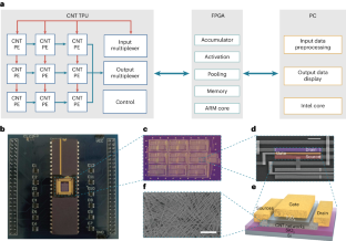
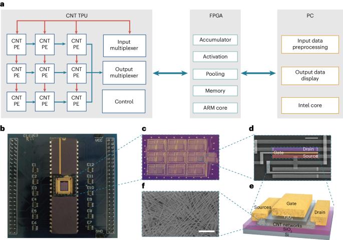
The growth of data-intensive computing tasks requires processing units with higher performance and energy efficiency, but these requirements are increasingly difficult to achieve with conventional semiconductor technology. One potential solution is to combine developments in devices with innovations in system architecture. Here we report a tensor processing unit (TPU) that is based on 3,000 carbon nanotube field-effect transistors and can perform energy-efficient convolution operations and matrix multiplication. The TPU is constructed with a systolic array architecture that allows parallel 2 bit integer multiply–accumulate operations. A five-layer convolutional neural network based on the TPU can perform MNIST image recognition with an accuracy of up to 88% for a power consumption of 295 µW. We use an optimized nanotube fabrication process that offers a semiconductor purity of 99.9999% and ultraclean surfaces, leading to transistors with high on-current densities and uniformity. Using system-level simulations, we estimate that an 8 bit TPU made with nanotube transistors at a 180 nm technology node could reach a main frequency of 850 MHz and an energy efficiency of 1 tera-operations per second per watt. Carbon nanotube networks made with high purity and ultraclean interfaces can be used to make a tensor processing unit that contains 3,000 transistors in a systolic array architecture to improve energy efficiency in accelerating neural network tasks.
期刊介绍:
Nature Electronics is a comprehensive journal that publishes both fundamental and applied research in the field of electronics. It encompasses a wide range of topics, including the study of new phenomena and devices, the design and construction of electronic circuits, and the practical applications of electronics. In addition, the journal explores the commercial and industrial aspects of electronics research.
The primary focus of Nature Electronics is on the development of technology and its potential impact on society. The journal incorporates the contributions of scientists, engineers, and industry professionals, offering a platform for their research findings. Moreover, Nature Electronics provides insightful commentary, thorough reviews, and analysis of the key issues that shape the field, as well as the technologies that are reshaping society.
Like all journals within the prestigious Nature brand, Nature Electronics upholds the highest standards of quality. It maintains a dedicated team of professional editors and follows a fair and rigorous peer-review process. The journal also ensures impeccable copy-editing and production, enabling swift publication. Additionally, Nature Electronics prides itself on its editorial independence, ensuring unbiased and impartial reporting.
In summary, Nature Electronics is a leading journal that publishes cutting-edge research in electronics. With its multidisciplinary approach and commitment to excellence, the journal serves as a valuable resource for scientists, engineers, and industry professionals seeking to stay at the forefront of advancements in the field.


 分享
分享
 求助内容:
求助内容: 应助结果提醒方式:
 扫码关注我们
