Felix V.E. Hensling, Patrick Vogt, Jisung Park, Shun-Li Shang, Huacheng Ye, Yu-Mi Wu, Kathleen Smith, Veronica Show, Kathy Azizie, Hanjong Paik, Debdeep Jena, Huili G. Xing, Y. Eren Suyolcu, Peter A. van Aken, Suman Datta, Zi-Kui Liu, Darrell G. Schlom
{"title":"利用亚氧化物分子束外延技术在生产线后端温度下制造全透明外延氧化物薄膜晶体管","authors":"Felix V.E. Hensling, Patrick Vogt, Jisung Park, Shun-Li Shang, Huacheng Ye, Yu-Mi Wu, Kathleen Smith, Veronica Show, Kathy Azizie, Hanjong Paik, Debdeep Jena, Huili G. Xing, Y. Eren Suyolcu, Peter A. van Aken, Suman Datta, Zi-Kui Liu, Darrell G. Schlom","doi":"10.1002/aelm.202400499","DOIUrl":null,"url":null,"abstract":"Transparent oxide thin film transistors (TFTs) are an important ingredient of transparent electronics. Their fabrication at the back-end-of-line (BEOL) opens the door to novel strategies to more closely integrate logic with memory for data-intensive computing architectures that overcome the scaling challenges of today's integrated circuits. A recently developed variant of molecular-beam epitaxy (MBE) called suboxide MBE (S-MBE) is demonstrated to be capable of growing epitaxial In<sub>2</sub>O<sub>3</sub> at BEOL temperatures with unmatched crystal quality. The fullwidth at halfmaximum of the rocking curve is 0.015° and, thus, ≈5x narrower than any reports at any temperature to date and limited by the substrate quality. The key to achieving these results is the provision of an In<sub>2</sub>O beam by S-MBE, which enables growth in adsorption control and is kinetically favorable. To benchmark this deposition method for TFTs, rudimentary devices were fabricated.","PeriodicalId":110,"journal":{"name":"Advanced Electronic Materials","volume":"59 1","pages":""},"PeriodicalIF":5.3000,"publicationDate":"2024-09-11","publicationTypes":"Journal Article","fieldsOfStudy":null,"isOpenAccess":false,"openAccessPdf":"","citationCount":"0","resultStr":"{\"title\":\"Fully Transparent Epitaxial Oxide Thin-Film Transistor Fabricated at Back-End-of-Line Temperature by Suboxide Molecular-Beam Epitaxy\",\"authors\":\"Felix V.E. Hensling, Patrick Vogt, Jisung Park, Shun-Li Shang, Huacheng Ye, Yu-Mi Wu, Kathleen Smith, Veronica Show, Kathy Azizie, Hanjong Paik, Debdeep Jena, Huili G. Xing, Y. Eren Suyolcu, Peter A. van Aken, Suman Datta, Zi-Kui Liu, Darrell G. Schlom\",\"doi\":\"10.1002/aelm.202400499\",\"DOIUrl\":null,\"url\":null,\"abstract\":\"Transparent oxide thin film transistors (TFTs) are an important ingredient of transparent electronics. Their fabrication at the back-end-of-line (BEOL) opens the door to novel strategies to more closely integrate logic with memory for data-intensive computing architectures that overcome the scaling challenges of today's integrated circuits. A recently developed variant of molecular-beam epitaxy (MBE) called suboxide MBE (S-MBE) is demonstrated to be capable of growing epitaxial In<sub>2</sub>O<sub>3</sub> at BEOL temperatures with unmatched crystal quality. The fullwidth at halfmaximum of the rocking curve is 0.015° and, thus, ≈5x narrower than any reports at any temperature to date and limited by the substrate quality. The key to achieving these results is the provision of an In<sub>2</sub>O beam by S-MBE, which enables growth in adsorption control and is kinetically favorable. To benchmark this deposition method for TFTs, rudimentary devices were fabricated.\",\"PeriodicalId\":110,\"journal\":{\"name\":\"Advanced Electronic Materials\",\"volume\":\"59 1\",\"pages\":\"\"},\"PeriodicalIF\":5.3000,\"publicationDate\":\"2024-09-11\",\"publicationTypes\":\"Journal Article\",\"fieldsOfStudy\":null,\"isOpenAccess\":false,\"openAccessPdf\":\"\",\"citationCount\":\"0\",\"resultStr\":null,\"platform\":\"Semanticscholar\",\"paperid\":null,\"PeriodicalName\":\"Advanced Electronic Materials\",\"FirstCategoryId\":\"88\",\"ListUrlMain\":\"https://doi.org/10.1002/aelm.202400499\",\"RegionNum\":2,\"RegionCategory\":\"材料科学\",\"ArticlePicture\":[],\"TitleCN\":null,\"AbstractTextCN\":null,\"PMCID\":null,\"EPubDate\":\"\",\"PubModel\":\"\",\"JCR\":\"Q2\",\"JCRName\":\"MATERIALS SCIENCE, MULTIDISCIPLINARY\",\"Score\":null,\"Total\":0}","platform":"Semanticscholar","paperid":null,"PeriodicalName":"Advanced Electronic Materials","FirstCategoryId":"88","ListUrlMain":"https://doi.org/10.1002/aelm.202400499","RegionNum":2,"RegionCategory":"材料科学","ArticlePicture":[],"TitleCN":null,"AbstractTextCN":null,"PMCID":null,"EPubDate":"","PubModel":"","JCR":"Q2","JCRName":"MATERIALS SCIENCE, MULTIDISCIPLINARY","Score":null,"Total":0}
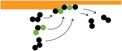
Fully Transparent Epitaxial Oxide Thin-Film Transistor Fabricated at Back-End-of-Line Temperature by Suboxide Molecular-Beam Epitaxy
Transparent oxide thin film transistors (TFTs) are an important ingredient of transparent electronics. Their fabrication at the back-end-of-line (BEOL) opens the door to novel strategies to more closely integrate logic with memory for data-intensive computing architectures that overcome the scaling challenges of today's integrated circuits. A recently developed variant of molecular-beam epitaxy (MBE) called suboxide MBE (S-MBE) is demonstrated to be capable of growing epitaxial In2O3 at BEOL temperatures with unmatched crystal quality. The fullwidth at halfmaximum of the rocking curve is 0.015° and, thus, ≈5x narrower than any reports at any temperature to date and limited by the substrate quality. The key to achieving these results is the provision of an In2O beam by S-MBE, which enables growth in adsorption control and is kinetically favorable. To benchmark this deposition method for TFTs, rudimentary devices were fabricated.
期刊介绍:
Advanced Electronic Materials is an interdisciplinary forum for peer-reviewed, high-quality, high-impact research in the fields of materials science, physics, and engineering of electronic and magnetic materials. It includes research on physics and physical properties of electronic and magnetic materials, spintronics, electronics, device physics and engineering, micro- and nano-electromechanical systems, and organic electronics, in addition to fundamental research.


 分享
分享
 求助内容:
求助内容: 应助结果提醒方式:
 扫码关注我们
