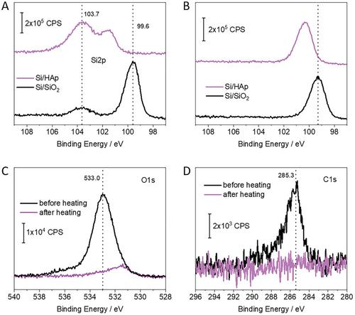
{"title":"矿物界面掺杂:在硅上沉积羟基磷灰石以触发电子特性","authors":"Peter Thissen, Roberto C. Longo","doi":"10.1002/admi.202400061","DOIUrl":null,"url":null,"abstract":"<p>Doping silicon wafers without using highly toxic or corrosive chemical substances has become a critical issue for semiconductor device manufacturing. In this work, ultra-thin films of hydroxyapatite (Ca<sub>5</sub>(PO<sub>4</sub>)<sub>3</sub>OH) are prepared by tethering by aggregation and growth (T-BAG), and further processed by spike annealing. Via in situ infrared (IR), the decomposition of hydroxyapatite and intermixing with the native silicon oxide is observed already at temperatures as low as 200 °C. Phosphate transport through the native silicon oxide is driven by a phase transformation into a more stable thermal oxide. At 700 °C, diffusion of phosphorus into the sub-surface region of oxide-free silicon is observed. In situ IR combined with electrical impedance spectroscopy (EIS), time-of-flight secondary ion mass spectrometry (ToF-SIMS), and X-ray photoelectron spectroscopy (XPS) measurements allows to conclude that the phosphorus is: i) transported through the silicon oxide barrier, ii)) diffused inside the oxide-free silicon, and iii) finally modified the electrical activity of the silicon wafer. To further explain the experimental findings, density-functional theory (DFT) is used to demonstrate the extent of the effect of phosphorus doping on the electronic nature of silicon surfaces, showing that even small amounts of doping can have a measurable effect on the electrical performance of semiconductor wafers.</p>","PeriodicalId":115,"journal":{"name":"Advanced Materials Interfaces","volume":"11 31","pages":""},"PeriodicalIF":4.4000,"publicationDate":"2024-09-12","publicationTypes":"Journal Article","fieldsOfStudy":null,"isOpenAccess":false,"openAccessPdf":"https://onlinelibrary.wiley.com/doi/epdf/10.1002/admi.202400061","citationCount":"0","resultStr":"{\"title\":\"Mineral Interface Doping: Hydroxyapatite Deposited on Silicon to Trigger the Electronic Properties\",\"authors\":\"Peter Thissen, Roberto C. Longo\",\"doi\":\"10.1002/admi.202400061\",\"DOIUrl\":null,\"url\":null,\"abstract\":\"<p>Doping silicon wafers without using highly toxic or corrosive chemical substances has become a critical issue for semiconductor device manufacturing. In this work, ultra-thin films of hydroxyapatite (Ca<sub>5</sub>(PO<sub>4</sub>)<sub>3</sub>OH) are prepared by tethering by aggregation and growth (T-BAG), and further processed by spike annealing. Via in situ infrared (IR), the decomposition of hydroxyapatite and intermixing with the native silicon oxide is observed already at temperatures as low as 200 °C. Phosphate transport through the native silicon oxide is driven by a phase transformation into a more stable thermal oxide. At 700 °C, diffusion of phosphorus into the sub-surface region of oxide-free silicon is observed. In situ IR combined with electrical impedance spectroscopy (EIS), time-of-flight secondary ion mass spectrometry (ToF-SIMS), and X-ray photoelectron spectroscopy (XPS) measurements allows to conclude that the phosphorus is: i) transported through the silicon oxide barrier, ii)) diffused inside the oxide-free silicon, and iii) finally modified the electrical activity of the silicon wafer. To further explain the experimental findings, density-functional theory (DFT) is used to demonstrate the extent of the effect of phosphorus doping on the electronic nature of silicon surfaces, showing that even small amounts of doping can have a measurable effect on the electrical performance of semiconductor wafers.</p>\",\"PeriodicalId\":115,\"journal\":{\"name\":\"Advanced Materials Interfaces\",\"volume\":\"11 31\",\"pages\":\"\"},\"PeriodicalIF\":4.4000,\"publicationDate\":\"2024-09-12\",\"publicationTypes\":\"Journal Article\",\"fieldsOfStudy\":null,\"isOpenAccess\":false,\"openAccessPdf\":\"https://onlinelibrary.wiley.com/doi/epdf/10.1002/admi.202400061\",\"citationCount\":\"0\",\"resultStr\":null,\"platform\":\"Semanticscholar\",\"paperid\":null,\"PeriodicalName\":\"Advanced Materials Interfaces\",\"FirstCategoryId\":\"88\",\"ListUrlMain\":\"https://advanced.onlinelibrary.wiley.com/doi/10.1002/admi.202400061\",\"RegionNum\":3,\"RegionCategory\":\"材料科学\",\"ArticlePicture\":[],\"TitleCN\":null,\"AbstractTextCN\":null,\"PMCID\":null,\"EPubDate\":\"\",\"PubModel\":\"\",\"JCR\":\"Q2\",\"JCRName\":\"CHEMISTRY, MULTIDISCIPLINARY\",\"Score\":null,\"Total\":0}","platform":"Semanticscholar","paperid":null,"PeriodicalName":"Advanced Materials Interfaces","FirstCategoryId":"88","ListUrlMain":"https://advanced.onlinelibrary.wiley.com/doi/10.1002/admi.202400061","RegionNum":3,"RegionCategory":"材料科学","ArticlePicture":[],"TitleCN":null,"AbstractTextCN":null,"PMCID":null,"EPubDate":"","PubModel":"","JCR":"Q2","JCRName":"CHEMISTRY, MULTIDISCIPLINARY","Score":null,"Total":0}
引用次数: 0
摘要
在不使用剧毒或腐蚀性化学物质的情况下对硅晶片进行掺杂已成为半导体设备制造的一个关键问题。在这项工作中,通过聚合和生长(T-BAG)法制备了羟基磷灰石(Ca5(PO4)3OH)超薄薄膜,并通过尖峰退火法进行了进一步处理。通过原位红外线(IR),在低至 200 °C 的温度下就能观察到羟基磷灰石的分解以及与原生氧化硅的混合。磷酸盐在原生氧化硅中的传输是由相变驱动的,相变后的氧化硅具有更稳定的热氧化性。在 700 ℃ 时,可以观察到磷扩散到无氧化物硅的次表面区域。原位红外光谱与电阻抗光谱 (EIS)、飞行时间二次离子质谱 (ToF-SIMS) 和 X 射线光电子能谱 (XPS) 测量相结合,得出了以下结论:i) 磷通过硅氧化物阻挡层传输;ii) 在无氧化物硅内部扩散;iii) 最终改变了硅晶片的电活性。为了进一步解释实验结果,我们使用密度泛函理论(DFT)来证明磷掺杂对硅表面电子性质的影响程度,结果表明即使少量的磷掺杂也会对半导体晶片的电性能产生可测量的影响。
Mineral Interface Doping: Hydroxyapatite Deposited on Silicon to Trigger the Electronic Properties
Doping silicon wafers without using highly toxic or corrosive chemical substances has become a critical issue for semiconductor device manufacturing. In this work, ultra-thin films of hydroxyapatite (Ca5(PO4)3OH) are prepared by tethering by aggregation and growth (T-BAG), and further processed by spike annealing. Via in situ infrared (IR), the decomposition of hydroxyapatite and intermixing with the native silicon oxide is observed already at temperatures as low as 200 °C. Phosphate transport through the native silicon oxide is driven by a phase transformation into a more stable thermal oxide. At 700 °C, diffusion of phosphorus into the sub-surface region of oxide-free silicon is observed. In situ IR combined with electrical impedance spectroscopy (EIS), time-of-flight secondary ion mass spectrometry (ToF-SIMS), and X-ray photoelectron spectroscopy (XPS) measurements allows to conclude that the phosphorus is: i) transported through the silicon oxide barrier, ii)) diffused inside the oxide-free silicon, and iii) finally modified the electrical activity of the silicon wafer. To further explain the experimental findings, density-functional theory (DFT) is used to demonstrate the extent of the effect of phosphorus doping on the electronic nature of silicon surfaces, showing that even small amounts of doping can have a measurable effect on the electrical performance of semiconductor wafers.
期刊介绍:
Advanced Materials Interfaces publishes top-level research on interface technologies and effects. Considering any interface formed between solids, liquids, and gases, the journal ensures an interdisciplinary blend of physics, chemistry, materials science, and life sciences. Advanced Materials Interfaces was launched in 2014 and received an Impact Factor of 4.834 in 2018.
The scope of Advanced Materials Interfaces is dedicated to interfaces and surfaces that play an essential role in virtually all materials and devices. Physics, chemistry, materials science and life sciences blend to encourage new, cross-pollinating ideas, which will drive forward our understanding of the processes at the interface.
Advanced Materials Interfaces covers all topics in interface-related research:
Oil / water separation,
Applications of nanostructured materials,
2D materials and heterostructures,
Surfaces and interfaces in organic electronic devices,
Catalysis and membranes,
Self-assembly and nanopatterned surfaces,
Composite and coating materials,
Biointerfaces for technical and medical applications.
Advanced Materials Interfaces provides a forum for topics on surface and interface science with a wide choice of formats: Reviews, Full Papers, and Communications, as well as Progress Reports and Research News.


 分享
分享
 求助内容:
求助内容: 应助结果提醒方式:
 扫码关注我们
