D. P. Radchenko, I. V. Zaporotskova, L. V. Kozhitov, P. A. Zaporotskov, A. V. Popkova, V. G. Kosushkin
{"title":"Simulation of the Radio Absorbing Properties of Pyrolyzed Polyacrylonitrile in the Frequency Range from 3 to 50 GHz","authors":"D. P. Radchenko, I. V. Zaporotskova, L. V. Kozhitov, P. A. Zaporotskov, A. V. Popkova, V. G. Kosushkin","doi":"10.1134/s1063739723080036","DOIUrl":null,"url":null,"abstract":"<h3 data-test=\"abstract-sub-heading\">\n<b>Abstract</b>—</h3><p>At present, the electromagnetic characteristics of various materials, including polymeric materials, are being widely studied with the aim of using them as radio-absorbing coatings in electronics products. One such material is pyrolyzed polyacrylonitrile (PPAN). This article considers a model of electromagnetic wave absorption by PPAN layers with electrical conductivity of 72 and 180 S/m and a layer width of 0.15 to 2 mm, including those containing a metal filler (the so-called PPAN-based metal composite), in the frequency range of 3–50 GHz. The experimental data are compared with the data obtained in the course of simulation in terms of parameters such as the reflection, transmission, and absorption indices. Modeling is done in the software package COMSOL Multiphysics.</p>","PeriodicalId":21534,"journal":{"name":"Russian Microelectronics","volume":"39 1","pages":""},"PeriodicalIF":0.0000,"publicationDate":"2024-03-05","publicationTypes":"Journal Article","fieldsOfStudy":null,"isOpenAccess":false,"openAccessPdf":"","citationCount":"0","resultStr":null,"platform":"Semanticscholar","paperid":null,"PeriodicalName":"Russian Microelectronics","FirstCategoryId":"1085","ListUrlMain":"https://doi.org/10.1134/s1063739723080036","RegionNum":0,"RegionCategory":null,"ArticlePicture":[],"TitleCN":null,"AbstractTextCN":null,"PMCID":null,"EPubDate":"","PubModel":"","JCR":"Q4","JCRName":"Engineering","Score":null,"Total":0}
引用次数: 0
Abstract—
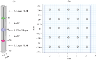
At present, the electromagnetic characteristics of various materials, including polymeric materials, are being widely studied with the aim of using them as radio-absorbing coatings in electronics products. One such material is pyrolyzed polyacrylonitrile (PPAN). This article considers a model of electromagnetic wave absorption by PPAN layers with electrical conductivity of 72 and 180 S/m and a layer width of 0.15 to 2 mm, including those containing a metal filler (the so-called PPAN-based metal composite), in the frequency range of 3–50 GHz. The experimental data are compared with the data obtained in the course of simulation in terms of parameters such as the reflection, transmission, and absorption indices. Modeling is done in the software package COMSOL Multiphysics.
期刊介绍:
Russian Microelectronics covers physical, technological, and some VLSI and ULSI circuit-technical aspects of microelectronics and nanoelectronics; it informs the reader of new trends in submicron optical, x-ray, electron, and ion-beam lithography technology; dry processing techniques, etching, doping; and deposition and planarization technology. Significant space is devoted to problems arising in the application of proton, electron, and ion beams, plasma, etc. Consideration is given to new equipment, including cluster tools and control in situ and submicron CMOS, bipolar, and BICMOS technologies. The journal publishes papers addressing problems of molecular beam epitaxy and related processes; heterojunction devices and integrated circuits; the technology and devices of nanoelectronics; and the fabrication of nanometer scale devices, including new device structures, quantum-effect devices, and superconducting devices. The reader will find papers containing news of the diagnostics of surfaces and microelectronic structures, the modeling of technological processes and devices in micro- and nanoelectronics, including nanotransistors, and solid state qubits.


 分享
分享
 求助内容:
求助内容: 应助结果提醒方式:
 扫码关注我们
