{"title":"Structure and Formation of Superflash Nonvolatile Memory Cells","authors":"D. A. Abdullaev, E. V. Bobrova, R. A. Milovanov","doi":"10.1134/s1063739724600249","DOIUrl":null,"url":null,"abstract":"<h3 data-test=\"abstract-sub-heading\">Abstract</h3><p>Split-gate embedded Flash memory technology has been around for decades and has become the standard application for a wide range of devices such as microcontrollers and smart cards. Among them, due to a number of advantages, SuperFlash (SF) produced by Silicon Storage Technology is the most widely used nonvolatile memory technology. In this paper, the results of a study of the structure of memory cells (MCs) are presented and the principle of their operation, as well as the main technological stages of the production process of forming transistor structures, is discussed.</p>","PeriodicalId":21534,"journal":{"name":"Russian Microelectronics","volume":"53 1","pages":""},"PeriodicalIF":0.0000,"publicationDate":"2024-07-26","publicationTypes":"Journal Article","fieldsOfStudy":null,"isOpenAccess":false,"openAccessPdf":"","citationCount":"0","resultStr":null,"platform":"Semanticscholar","paperid":null,"PeriodicalName":"Russian Microelectronics","FirstCategoryId":"1085","ListUrlMain":"https://doi.org/10.1134/s1063739724600249","RegionNum":0,"RegionCategory":null,"ArticlePicture":[],"TitleCN":null,"AbstractTextCN":null,"PMCID":null,"EPubDate":"","PubModel":"","JCR":"Q4","JCRName":"Engineering","Score":null,"Total":0}
引用次数: 0
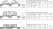
Abstract
Split-gate embedded Flash memory technology has been around for decades and has become the standard application for a wide range of devices such as microcontrollers and smart cards. Among them, due to a number of advantages, SuperFlash (SF) produced by Silicon Storage Technology is the most widely used nonvolatile memory technology. In this paper, the results of a study of the structure of memory cells (MCs) are presented and the principle of their operation, as well as the main technological stages of the production process of forming transistor structures, is discussed.
期刊介绍:
Russian Microelectronics covers physical, technological, and some VLSI and ULSI circuit-technical aspects of microelectronics and nanoelectronics; it informs the reader of new trends in submicron optical, x-ray, electron, and ion-beam lithography technology; dry processing techniques, etching, doping; and deposition and planarization technology. Significant space is devoted to problems arising in the application of proton, electron, and ion beams, plasma, etc. Consideration is given to new equipment, including cluster tools and control in situ and submicron CMOS, bipolar, and BICMOS technologies. The journal publishes papers addressing problems of molecular beam epitaxy and related processes; heterojunction devices and integrated circuits; the technology and devices of nanoelectronics; and the fabrication of nanometer scale devices, including new device structures, quantum-effect devices, and superconducting devices. The reader will find papers containing news of the diagnostics of surfaces and microelectronic structures, the modeling of technological processes and devices in micro- and nanoelectronics, including nanotransistors, and solid state qubits.


 分享
分享
 求助内容:
求助内容: 应助结果提醒方式:
 扫码关注我们
