{"title":"Ion-Assisted Magnetron Deposition of AlN Films","authors":"R. V. Selyukov, V. V. Naumov","doi":"10.1134/s1063739723600309","DOIUrl":null,"url":null,"abstract":"<h3 data-test=\"abstract-sub-heading\">Abstract</h3><p>AlN films are prepared by reactive magnetron sputtering at a floating potential and at the bias –15 V on the substrate. It is found that ion-assisted deposition facilitates the formation of fiber texture AlN (104). This result can be explained by generation of compressive stress in films due to ion bombardment and preferred orientation (104) is favored for stressed films minimizing the elastic strain energy. Ion-assisted deposition provides dense and large-grained structure of AlN films due to high adatom mobility.</p>","PeriodicalId":21534,"journal":{"name":"Russian Microelectronics","volume":"14 1","pages":""},"PeriodicalIF":0.0000,"publicationDate":"2024-03-21","publicationTypes":"Journal Article","fieldsOfStudy":null,"isOpenAccess":false,"openAccessPdf":"","citationCount":"0","resultStr":null,"platform":"Semanticscholar","paperid":null,"PeriodicalName":"Russian Microelectronics","FirstCategoryId":"1085","ListUrlMain":"https://doi.org/10.1134/s1063739723600309","RegionNum":0,"RegionCategory":null,"ArticlePicture":[],"TitleCN":null,"AbstractTextCN":null,"PMCID":null,"EPubDate":"","PubModel":"","JCR":"Q4","JCRName":"Engineering","Score":null,"Total":0}
引用次数: 0
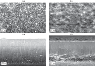
Abstract
AlN films are prepared by reactive magnetron sputtering at a floating potential and at the bias –15 V on the substrate. It is found that ion-assisted deposition facilitates the formation of fiber texture AlN (104). This result can be explained by generation of compressive stress in films due to ion bombardment and preferred orientation (104) is favored for stressed films minimizing the elastic strain energy. Ion-assisted deposition provides dense and large-grained structure of AlN films due to high adatom mobility.
期刊介绍:
Russian Microelectronics covers physical, technological, and some VLSI and ULSI circuit-technical aspects of microelectronics and nanoelectronics; it informs the reader of new trends in submicron optical, x-ray, electron, and ion-beam lithography technology; dry processing techniques, etching, doping; and deposition and planarization technology. Significant space is devoted to problems arising in the application of proton, electron, and ion beams, plasma, etc. Consideration is given to new equipment, including cluster tools and control in situ and submicron CMOS, bipolar, and BICMOS technologies. The journal publishes papers addressing problems of molecular beam epitaxy and related processes; heterojunction devices and integrated circuits; the technology and devices of nanoelectronics; and the fabrication of nanometer scale devices, including new device structures, quantum-effect devices, and superconducting devices. The reader will find papers containing news of the diagnostics of surfaces and microelectronic structures, the modeling of technological processes and devices in micro- and nanoelectronics, including nanotransistors, and solid state qubits.


 分享
分享
 求助内容:
求助内容: 应助结果提醒方式:
 扫码关注我们
