{"title":"Investigation of the Features of Metallization Formation for N-MOS Transistor Structures with a Vertical Channel","authors":"V. S. Gornostay-Polsky, V. I. Shevyakov","doi":"10.1134/s1063739723600310","DOIUrl":null,"url":null,"abstract":"<h3 data-test=\"abstract-sub-heading\">Abstract—</h3><p>This paper examines the features of the metallization unit of a power transistor with a vertical channel. It consists of alternating layers based on depth and includes titanium, titanium nitride and tungsten. Thick-film aluminum wiring is placed on the surface of the silicon substrate. Based on Auger spectroscopy and analysis of transmission electron diffraction patterns, it was revealed that a titanium dislicide film in the C<sub>54</sub> phase is formed using low-temperature heat treatment and subsequent high-temperature annealing. It is shown that the introduction of special cyclic plasma treatment after deposition of a layer of titanium nitride using the metal-organic chemical vapor deposition method (MOCVD) made it possible to reduce the resistance of the films and reduce the level of mechanical stress. It has been shown that the addition of rhenium, titanium and nitrogen in the range of 5–10 at % allows you to reduce the mechanical stress of the tungsten layer by 3–5 times. Depending on the method of deposition of tungsten (magnetron or chemical), we have proposed two design options for this unit. A method for forming aluminum wiring based on thick-film aluminum using a sacrificial layer of titanium nitride is proposed. The proposed solutions provide the opportunity to improve the electrical and mechanical properties of the metallization unit of MIS transistor structures with a vertical channel.</p>","PeriodicalId":21534,"journal":{"name":"Russian Microelectronics","volume":"29 1","pages":""},"PeriodicalIF":0.0000,"publicationDate":"2024-03-21","publicationTypes":"Journal Article","fieldsOfStudy":null,"isOpenAccess":false,"openAccessPdf":"","citationCount":"0","resultStr":null,"platform":"Semanticscholar","paperid":null,"PeriodicalName":"Russian Microelectronics","FirstCategoryId":"1085","ListUrlMain":"https://doi.org/10.1134/s1063739723600310","RegionNum":0,"RegionCategory":null,"ArticlePicture":[],"TitleCN":null,"AbstractTextCN":null,"PMCID":null,"EPubDate":"","PubModel":"","JCR":"Q4","JCRName":"Engineering","Score":null,"Total":0}
引用次数: 0
Abstract
Abstract—
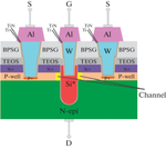
This paper examines the features of the metallization unit of a power transistor with a vertical channel. It consists of alternating layers based on depth and includes titanium, titanium nitride and tungsten. Thick-film aluminum wiring is placed on the surface of the silicon substrate. Based on Auger spectroscopy and analysis of transmission electron diffraction patterns, it was revealed that a titanium dislicide film in the C54 phase is formed using low-temperature heat treatment and subsequent high-temperature annealing. It is shown that the introduction of special cyclic plasma treatment after deposition of a layer of titanium nitride using the metal-organic chemical vapor deposition method (MOCVD) made it possible to reduce the resistance of the films and reduce the level of mechanical stress. It has been shown that the addition of rhenium, titanium and nitrogen in the range of 5–10 at % allows you to reduce the mechanical stress of the tungsten layer by 3–5 times. Depending on the method of deposition of tungsten (magnetron or chemical), we have proposed two design options for this unit. A method for forming aluminum wiring based on thick-film aluminum using a sacrificial layer of titanium nitride is proposed. The proposed solutions provide the opportunity to improve the electrical and mechanical properties of the metallization unit of MIS transistor structures with a vertical channel.
期刊介绍:
Russian Microelectronics covers physical, technological, and some VLSI and ULSI circuit-technical aspects of microelectronics and nanoelectronics; it informs the reader of new trends in submicron optical, x-ray, electron, and ion-beam lithography technology; dry processing techniques, etching, doping; and deposition and planarization technology. Significant space is devoted to problems arising in the application of proton, electron, and ion beams, plasma, etc. Consideration is given to new equipment, including cluster tools and control in situ and submicron CMOS, bipolar, and BICMOS technologies. The journal publishes papers addressing problems of molecular beam epitaxy and related processes; heterojunction devices and integrated circuits; the technology and devices of nanoelectronics; and the fabrication of nanometer scale devices, including new device structures, quantum-effect devices, and superconducting devices. The reader will find papers containing news of the diagnostics of surfaces and microelectronic structures, the modeling of technological processes and devices in micro- and nanoelectronics, including nanotransistors, and solid state qubits.


 分享
分享
 求助内容:
求助内容: 应助结果提醒方式:
 扫码关注我们
