{"title":"Technique of Time Depend Dielectric Breakdown for the Wafer-Level Testing of Thin Dielectrics of MIS Devices","authors":"D. V. Andreev, V. M. Maslovsky, V. V. Andreev","doi":"10.1134/s1063739723600450","DOIUrl":null,"url":null,"abstract":"<h3 data-test=\"abstract-sub-heading\">Abstract—</h3><p>The paper proposes a novel technique of time depend dielectric breakdown for the wafer-level testing of thin dielectric of MIS devices based on concatenation of J-Ramp and Bounded J-Ramp methods. The suggested method enhances the existing method capabilities by introducing measurement injection modes. When DUT is under the measurement mode, the charge injection into the gate dielectric is realized under constant current density <i>J</i><sub>m</sub> at which any significant charge degradation of dielectric is not observed. Introduction of the measurement modes give an opportunity to monitor a change of the charge state of thin gate dielectric during all the test. The suggested test is started similar to Bounded J-Ramp method and then in order to raise the monitoring speed, the value of bounded current <i>J</i><sub>b</sub> could be step wisely increased over certain time intervals which are much longer in time in comparison with J-Ramp method. As a result, the charge injection into the gate dielectric could be implemented under multiple <i>J</i><sub>b</sub> values. This test algorithm gives an opportunity to greatly enhance functional capabilities of the existing test methods and the suggested technique raises speed to test.</p>","PeriodicalId":21534,"journal":{"name":"Russian Microelectronics","volume":"55 1","pages":""},"PeriodicalIF":0.0000,"publicationDate":"2024-03-21","publicationTypes":"Journal Article","fieldsOfStudy":null,"isOpenAccess":false,"openAccessPdf":"","citationCount":"0","resultStr":null,"platform":"Semanticscholar","paperid":null,"PeriodicalName":"Russian Microelectronics","FirstCategoryId":"1085","ListUrlMain":"https://doi.org/10.1134/s1063739723600450","RegionNum":0,"RegionCategory":null,"ArticlePicture":[],"TitleCN":null,"AbstractTextCN":null,"PMCID":null,"EPubDate":"","PubModel":"","JCR":"Q4","JCRName":"Engineering","Score":null,"Total":0}
引用次数: 0
Abstract
Abstract—
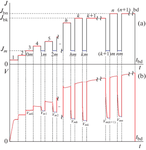
The paper proposes a novel technique of time depend dielectric breakdown for the wafer-level testing of thin dielectric of MIS devices based on concatenation of J-Ramp and Bounded J-Ramp methods. The suggested method enhances the existing method capabilities by introducing measurement injection modes. When DUT is under the measurement mode, the charge injection into the gate dielectric is realized under constant current density Jm at which any significant charge degradation of dielectric is not observed. Introduction of the measurement modes give an opportunity to monitor a change of the charge state of thin gate dielectric during all the test. The suggested test is started similar to Bounded J-Ramp method and then in order to raise the monitoring speed, the value of bounded current Jb could be step wisely increased over certain time intervals which are much longer in time in comparison with J-Ramp method. As a result, the charge injection into the gate dielectric could be implemented under multiple Jb values. This test algorithm gives an opportunity to greatly enhance functional capabilities of the existing test methods and the suggested technique raises speed to test.
期刊介绍:
Russian Microelectronics covers physical, technological, and some VLSI and ULSI circuit-technical aspects of microelectronics and nanoelectronics; it informs the reader of new trends in submicron optical, x-ray, electron, and ion-beam lithography technology; dry processing techniques, etching, doping; and deposition and planarization technology. Significant space is devoted to problems arising in the application of proton, electron, and ion beams, plasma, etc. Consideration is given to new equipment, including cluster tools and control in situ and submicron CMOS, bipolar, and BICMOS technologies. The journal publishes papers addressing problems of molecular beam epitaxy and related processes; heterojunction devices and integrated circuits; the technology and devices of nanoelectronics; and the fabrication of nanometer scale devices, including new device structures, quantum-effect devices, and superconducting devices. The reader will find papers containing news of the diagnostics of surfaces and microelectronic structures, the modeling of technological processes and devices in micro- and nanoelectronics, including nanotransistors, and solid state qubits.


 分享
分享
 求助内容:
求助内容: 应助结果提醒方式:
 扫码关注我们
