{"title":"Electrostatic-Assisted Ultrasonic Spray-Coating for Nanotechnology Applications","authors":"V. Petukhov, N. Struchkov, V. Nevolin","doi":"10.1134/s1063739723600681","DOIUrl":null,"url":null,"abstract":"<h3 data-test=\"abstract-sub-heading\">Abstract</h3><p>In this work we show a setup and optimized process of ultrasonic spray and electrostatic-assisted deposition of photoresist onto silicon substrates with deep etched areas. Drop size reduction at applied electric field is shown. The deposition of FP-3515 photoresist is conducted at a temperature of 45°C and provides good photoresist transfer and good film cleanness and quality. Deposition and drying of the photoresist layer is conducted simultaneously which implies uniform drying of the film and, thus, absence of mechanical strain. Another advantage is a possibility to create multi-layer coatings without partial dissolution of previously deposited layer. Deposited photoresist layer forms conformal film at edges and walls of deep etched silicon substrate. Maskless laser lithography has been conducted successfully that proved process practical suitability.</p>","PeriodicalId":21534,"journal":{"name":"Russian Microelectronics","volume":"52 1","pages":""},"PeriodicalIF":0.0000,"publicationDate":"2024-03-21","publicationTypes":"Journal Article","fieldsOfStudy":null,"isOpenAccess":false,"openAccessPdf":"","citationCount":"0","resultStr":null,"platform":"Semanticscholar","paperid":null,"PeriodicalName":"Russian Microelectronics","FirstCategoryId":"1085","ListUrlMain":"https://doi.org/10.1134/s1063739723600681","RegionNum":0,"RegionCategory":null,"ArticlePicture":[],"TitleCN":null,"AbstractTextCN":null,"PMCID":null,"EPubDate":"","PubModel":"","JCR":"Q4","JCRName":"Engineering","Score":null,"Total":0}
引用次数: 0
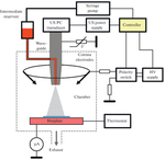
Abstract
In this work we show a setup and optimized process of ultrasonic spray and electrostatic-assisted deposition of photoresist onto silicon substrates with deep etched areas. Drop size reduction at applied electric field is shown. The deposition of FP-3515 photoresist is conducted at a temperature of 45°C and provides good photoresist transfer and good film cleanness and quality. Deposition and drying of the photoresist layer is conducted simultaneously which implies uniform drying of the film and, thus, absence of mechanical strain. Another advantage is a possibility to create multi-layer coatings without partial dissolution of previously deposited layer. Deposited photoresist layer forms conformal film at edges and walls of deep etched silicon substrate. Maskless laser lithography has been conducted successfully that proved process practical suitability.
期刊介绍:
Russian Microelectronics covers physical, technological, and some VLSI and ULSI circuit-technical aspects of microelectronics and nanoelectronics; it informs the reader of new trends in submicron optical, x-ray, electron, and ion-beam lithography technology; dry processing techniques, etching, doping; and deposition and planarization technology. Significant space is devoted to problems arising in the application of proton, electron, and ion beams, plasma, etc. Consideration is given to new equipment, including cluster tools and control in situ and submicron CMOS, bipolar, and BICMOS technologies. The journal publishes papers addressing problems of molecular beam epitaxy and related processes; heterojunction devices and integrated circuits; the technology and devices of nanoelectronics; and the fabrication of nanometer scale devices, including new device structures, quantum-effect devices, and superconducting devices. The reader will find papers containing news of the diagnostics of surfaces and microelectronic structures, the modeling of technological processes and devices in micro- and nanoelectronics, including nanotransistors, and solid state qubits.


 分享
分享
 求助内容:
求助内容: 应助结果提醒方式:
 扫码关注我们
