{"title":"Application of the Finite Element Method for Calculating Parameters of Surface Acoustic Waves and Devices Based on Them","authors":"A. S. Koigerov","doi":"10.1134/s1063739724700781","DOIUrl":null,"url":null,"abstract":"<h3 data-test=\"abstract-sub-heading\">Abstract</h3><p>A series of models based on the finite element method (FEM) for analyzing the parameters of surface acoustic waves (SAWs) and devices based on them are described. The computer method for generating models in the COMSOL Multiphysics program is described in a generalized form. The work in three main solvers in the COMSOL environment—the stationary mode, eigenfrequency domain, and frequency domain—is described and graphically illustrated. The properties of Rayleigh waves and leaky SAWs are analyzed. A visualization of a number of characteristics is presented. The analysis of parameters such as the phase velocity of the wave, electromechanical coupling coefficient, and static capacitance of the transducer is considered. The examples consider an equidistant transducer, a transducer with split electrodes, and a unidirectional transducer of the DART type. Methods for analyzing harmonics in SAWs and the waveguide effect are proposed. It is shown that the model is valid for both single-crystal substrates and layered structures. The analysis of the temperature coefficient of the frequency for structures as such TCSAW (temperature-compensated SAW) and I.H.P.SAW (incredible high-performance SAW) is considered. A model for calculating the amplitude-frequency responses of devices is presented. It is shown that the data obtained as a result of the numerical analysis correspond to the experimental data and known published sources.</p>","PeriodicalId":21534,"journal":{"name":"Russian Microelectronics","volume":"118 1","pages":""},"PeriodicalIF":0.0000,"publicationDate":"2024-06-04","publicationTypes":"Journal Article","fieldsOfStudy":null,"isOpenAccess":false,"openAccessPdf":"","citationCount":"0","resultStr":null,"platform":"Semanticscholar","paperid":null,"PeriodicalName":"Russian Microelectronics","FirstCategoryId":"1085","ListUrlMain":"https://doi.org/10.1134/s1063739724700781","RegionNum":0,"RegionCategory":null,"ArticlePicture":[],"TitleCN":null,"AbstractTextCN":null,"PMCID":null,"EPubDate":"","PubModel":"","JCR":"Q4","JCRName":"Engineering","Score":null,"Total":0}
引用次数: 0
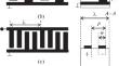
Abstract
A series of models based on the finite element method (FEM) for analyzing the parameters of surface acoustic waves (SAWs) and devices based on them are described. The computer method for generating models in the COMSOL Multiphysics program is described in a generalized form. The work in three main solvers in the COMSOL environment—the stationary mode, eigenfrequency domain, and frequency domain—is described and graphically illustrated. The properties of Rayleigh waves and leaky SAWs are analyzed. A visualization of a number of characteristics is presented. The analysis of parameters such as the phase velocity of the wave, electromechanical coupling coefficient, and static capacitance of the transducer is considered. The examples consider an equidistant transducer, a transducer with split electrodes, and a unidirectional transducer of the DART type. Methods for analyzing harmonics in SAWs and the waveguide effect are proposed. It is shown that the model is valid for both single-crystal substrates and layered structures. The analysis of the temperature coefficient of the frequency for structures as such TCSAW (temperature-compensated SAW) and I.H.P.SAW (incredible high-performance SAW) is considered. A model for calculating the amplitude-frequency responses of devices is presented. It is shown that the data obtained as a result of the numerical analysis correspond to the experimental data and known published sources.
期刊介绍:
Russian Microelectronics covers physical, technological, and some VLSI and ULSI circuit-technical aspects of microelectronics and nanoelectronics; it informs the reader of new trends in submicron optical, x-ray, electron, and ion-beam lithography technology; dry processing techniques, etching, doping; and deposition and planarization technology. Significant space is devoted to problems arising in the application of proton, electron, and ion beams, plasma, etc. Consideration is given to new equipment, including cluster tools and control in situ and submicron CMOS, bipolar, and BICMOS technologies. The journal publishes papers addressing problems of molecular beam epitaxy and related processes; heterojunction devices and integrated circuits; the technology and devices of nanoelectronics; and the fabrication of nanometer scale devices, including new device structures, quantum-effect devices, and superconducting devices. The reader will find papers containing news of the diagnostics of surfaces and microelectronic structures, the modeling of technological processes and devices in micro- and nanoelectronics, including nanotransistors, and solid state qubits.


 分享
分享
 求助内容:
求助内容: 应助结果提醒方式:
 扫码关注我们
