A. S. Gusev, A. O. Sultanov, A. V. Katkov, S. M. Ryndya, N. V. Siglovaya, A. N. Klochkov, R. V. Ryzhuk, N. I. Kargin, D. P. Borisenko
{"title":"Analysis of Carrier Scattering Mechanisms in AlN/GaN HEMT Heterostructures with an Ultrathin AlN Barrier","authors":"A. S. Gusev, A. O. Sultanov, A. V. Katkov, S. M. Ryndya, N. V. Siglovaya, A. N. Klochkov, R. V. Ryzhuk, N. I. Kargin, D. P. Borisenko","doi":"10.1134/s1063739724600304","DOIUrl":null,"url":null,"abstract":"<h3 data-test=\"abstract-sub-heading\">Abstract</h3><p>Using the method of molecular beam epitaxy with the plasma activation of nitrogen, experimental AlN/GaN heterostructures (HSs) with an ultrathin AlN barrier are obtained<i>.</i> The layer resistance of the optimized structures is less than 230 Ω/□. The scattering processes that limit the mobility of a two-dimensional electron gas (2DEG) in undoped AlN/GaN HSs with an ultrathin AlN barrier are studied. It is shown that in the range of <i>n</i><sub><i>s</i></sub> characteristic for AlN/GaN HEMT HSs (<i>n</i><sub>s</sub> > 1 × 10<sup>13</sup> cm<sup>–2</sup>), a noticeable contribution to the scattering of charge carriers is made by the roughness of the heterointerface.</p>","PeriodicalId":21534,"journal":{"name":"Russian Microelectronics","volume":"245 1","pages":""},"PeriodicalIF":0.0000,"publicationDate":"2024-07-26","publicationTypes":"Journal Article","fieldsOfStudy":null,"isOpenAccess":false,"openAccessPdf":"","citationCount":"0","resultStr":null,"platform":"Semanticscholar","paperid":null,"PeriodicalName":"Russian Microelectronics","FirstCategoryId":"1085","ListUrlMain":"https://doi.org/10.1134/s1063739724600304","RegionNum":0,"RegionCategory":null,"ArticlePicture":[],"TitleCN":null,"AbstractTextCN":null,"PMCID":null,"EPubDate":"","PubModel":"","JCR":"Q4","JCRName":"Engineering","Score":null,"Total":0}
引用次数: 0
Abstract
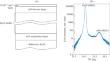
Using the method of molecular beam epitaxy with the plasma activation of nitrogen, experimental AlN/GaN heterostructures (HSs) with an ultrathin AlN barrier are obtained. The layer resistance of the optimized structures is less than 230 Ω/□. The scattering processes that limit the mobility of a two-dimensional electron gas (2DEG) in undoped AlN/GaN HSs with an ultrathin AlN barrier are studied. It is shown that in the range of ns characteristic for AlN/GaN HEMT HSs (ns > 1 × 1013 cm–2), a noticeable contribution to the scattering of charge carriers is made by the roughness of the heterointerface.
期刊介绍:
Russian Microelectronics covers physical, technological, and some VLSI and ULSI circuit-technical aspects of microelectronics and nanoelectronics; it informs the reader of new trends in submicron optical, x-ray, electron, and ion-beam lithography technology; dry processing techniques, etching, doping; and deposition and planarization technology. Significant space is devoted to problems arising in the application of proton, electron, and ion beams, plasma, etc. Consideration is given to new equipment, including cluster tools and control in situ and submicron CMOS, bipolar, and BICMOS technologies. The journal publishes papers addressing problems of molecular beam epitaxy and related processes; heterojunction devices and integrated circuits; the technology and devices of nanoelectronics; and the fabrication of nanometer scale devices, including new device structures, quantum-effect devices, and superconducting devices. The reader will find papers containing news of the diagnostics of surfaces and microelectronic structures, the modeling of technological processes and devices in micro- and nanoelectronics, including nanotransistors, and solid state qubits.


 分享
分享
 求助内容:
求助内容: 应助结果提醒方式:
 扫码关注我们
