{"title":"Controllable growth of wafer-scale two-dimensional PdS2xSe2(1-x) nanofilms with fully tunable compositions for high-performance photodetectors","authors":"Huan Zhou, Yulong Hao, Chen Fan, Shiwei Zhang, Chen Wang, Kaiyi Wang, Jie Zhou, Shijie Hao, Ting Shu, Xuemei Lu, Bo Li, Yongqiang Yu, Guolin Hao","doi":"10.1016/j.jmst.2024.12.036","DOIUrl":null,"url":null,"abstract":"Two-dimensional (2D) noble transition-metal dichalcogenide materials (NTMDs) have garnered remarkable attention due to their intriguing properties exhibiting potential applications in nanoelectronics, optoelectronics, and photonics. The electronic structure and physical properties of 2D NTMDs can be effectively modulated using alloy engineering strategy. Nevertheless, the precise growth of wafer-scale 2D NTMDs alloys remains a significant challenge. In this work, we have achieved the controllable preparation of wafer-scale (2-inch) 2D PdS<sub>2</sub><em><sub>x</sub></em>Se<sub>2(1-</sub><em><sub>x</sub></em><sub>)</sub> nanofilms (NFs) with fully tunable compositions on various substrates using pre-deposited Pd NFs assisted chemical vapor deposition technique. High-performance photodetectors based on the PdS<sub>2</sub><em><sub>x</sub></em>Se<sub>2(1-</sub><em><sub>x</sub></em><sub>)</sub> NFs were fabricated, which exhibit broadband photodetection performance from visible to near-infrared (NIR) wavelength range at room temperature. Significantly, the PdS<sub>0.9</sub>Se<sub>1.1</sub>-based photodetectors display a responsivity up to 0.192 A W<sup>−1</sup> and a large specific detectivity of 5.5 × 10<sup>11</sup> Jones for 850 nm light, enabling an excellent high-resolution NIR single-pixel imaging (SPI) without an additional filtering circuit. Our work paves a new route for the controlled synthesis of wafer-scale and high-quality 2D NTMDs alloy NFs, which is essential for designing advanced optoelectronic devices.","PeriodicalId":16154,"journal":{"name":"Journal of Materials Science & Technology","volume":"164 1","pages":""},"PeriodicalIF":14.3000,"publicationDate":"2025-02-06","publicationTypes":"Journal Article","fieldsOfStudy":null,"isOpenAccess":false,"openAccessPdf":"","citationCount":"0","resultStr":null,"platform":"Semanticscholar","paperid":null,"PeriodicalName":"Journal of Materials Science & Technology","FirstCategoryId":"88","ListUrlMain":"https://doi.org/10.1016/j.jmst.2024.12.036","RegionNum":1,"RegionCategory":"材料科学","ArticlePicture":[],"TitleCN":null,"AbstractTextCN":null,"PMCID":null,"EPubDate":"","PubModel":"","JCR":"Q1","JCRName":"MATERIALS SCIENCE, MULTIDISCIPLINARY","Score":null,"Total":0}
引用次数: 0
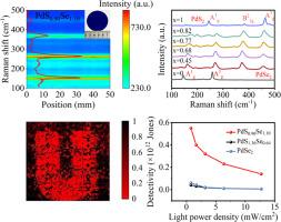
Abstract
Two-dimensional (2D) noble transition-metal dichalcogenide materials (NTMDs) have garnered remarkable attention due to their intriguing properties exhibiting potential applications in nanoelectronics, optoelectronics, and photonics. The electronic structure and physical properties of 2D NTMDs can be effectively modulated using alloy engineering strategy. Nevertheless, the precise growth of wafer-scale 2D NTMDs alloys remains a significant challenge. In this work, we have achieved the controllable preparation of wafer-scale (2-inch) 2D PdS2xSe2(1-x) nanofilms (NFs) with fully tunable compositions on various substrates using pre-deposited Pd NFs assisted chemical vapor deposition technique. High-performance photodetectors based on the PdS2xSe2(1-x) NFs were fabricated, which exhibit broadband photodetection performance from visible to near-infrared (NIR) wavelength range at room temperature. Significantly, the PdS0.9Se1.1-based photodetectors display a responsivity up to 0.192 A W−1 and a large specific detectivity of 5.5 × 10¹¹ Jones for 850 nm light, enabling an excellent high-resolution NIR single-pixel imaging (SPI) without an additional filtering circuit. Our work paves a new route for the controlled synthesis of wafer-scale and high-quality 2D NTMDs alloy NFs, which is essential for designing advanced optoelectronic devices.
期刊介绍:
Journal of Materials Science & Technology strives to promote global collaboration in the field of materials science and technology. It primarily publishes original research papers, invited review articles, letters, research notes, and summaries of scientific achievements. The journal covers a wide range of materials science and technology topics, including metallic materials, inorganic nonmetallic materials, and composite materials.


 分享
分享
 求助内容:
求助内容: 应助结果提醒方式:
 扫码关注我们
