Claire C. Onsager, Lev Rovinsky, Can C. Aygen, Shira K. Cohen, Noa Lachman, Matthew A. Grayson
{"title":"Getting Under the Sensor's Skin: The Importance of Electrical Contact Characterization for Conductive Composite Elastomers","authors":"Claire C. Onsager, Lev Rovinsky, Can C. Aygen, Shira K. Cohen, Noa Lachman, Matthew A. Grayson","doi":"10.1002/aelm.202400848","DOIUrl":null,"url":null,"abstract":"<p>Conductive elastomer composites can be used as flexible, lightweight, and inexpensive sensors, but they require ohmic electrical contacts to ensure readout consistency, and such contacts can suffer from hysteresis, non-ohmic behavior, and cyclic fatigue. This work investigates a common cause of non-ohmic conduction in such composite contacts, namely the thin insulating layer native to the surface of most silicone rubber composites that have been infused with multi-walled carbon nanotubes for piezoresistive sensing. Voltage sweep dc measurements of individual contacts on this surface layer behave as parallel head-to-tail diodes with asymmetric hysteresis. Frequency sweep ac measurements quantify the insulator thickness with a leaky capacitor model to be ∼1 µm, independent of nanotube concentration, much thicker than the apparent layer thickness as imaged with scanning electron microscopy. This analysis also confirms highly anisotropic bulk conduction, circa 100 times higher in-plane than cross-plane. To remove the surface layer, a simple surface abrasion is shown to achieve deep ohmic electrical contact to the elastomer bulk. A three-terminal method for verifying ohmic contacts is demonstrated and works even when all contacts are non-ohmic. This three-terminal method be easily applied to other conductive polymers for contact quality-testing.</p>","PeriodicalId":110,"journal":{"name":"Advanced Electronic Materials","volume":"11 5","pages":""},"PeriodicalIF":5.3000,"publicationDate":"2025-02-09","publicationTypes":"Journal Article","fieldsOfStudy":null,"isOpenAccess":false,"openAccessPdf":"https://onlinelibrary.wiley.com/doi/epdf/10.1002/aelm.202400848","citationCount":"0","resultStr":null,"platform":"Semanticscholar","paperid":null,"PeriodicalName":"Advanced Electronic Materials","FirstCategoryId":"88","ListUrlMain":"https://advanced.onlinelibrary.wiley.com/doi/10.1002/aelm.202400848","RegionNum":2,"RegionCategory":"材料科学","ArticlePicture":[],"TitleCN":null,"AbstractTextCN":null,"PMCID":null,"EPubDate":"","PubModel":"","JCR":"Q2","JCRName":"MATERIALS SCIENCE, MULTIDISCIPLINARY","Score":null,"Total":0}
引用次数: 0
Abstract
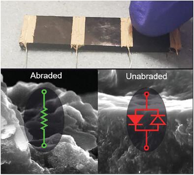
Conductive elastomer composites can be used as flexible, lightweight, and inexpensive sensors, but they require ohmic electrical contacts to ensure readout consistency, and such contacts can suffer from hysteresis, non-ohmic behavior, and cyclic fatigue. This work investigates a common cause of non-ohmic conduction in such composite contacts, namely the thin insulating layer native to the surface of most silicone rubber composites that have been infused with multi-walled carbon nanotubes for piezoresistive sensing. Voltage sweep dc measurements of individual contacts on this surface layer behave as parallel head-to-tail diodes with asymmetric hysteresis. Frequency sweep ac measurements quantify the insulator thickness with a leaky capacitor model to be ∼1 µm, independent of nanotube concentration, much thicker than the apparent layer thickness as imaged with scanning electron microscopy. This analysis also confirms highly anisotropic bulk conduction, circa 100 times higher in-plane than cross-plane. To remove the surface layer, a simple surface abrasion is shown to achieve deep ohmic electrical contact to the elastomer bulk. A three-terminal method for verifying ohmic contacts is demonstrated and works even when all contacts are non-ohmic. This three-terminal method be easily applied to other conductive polymers for contact quality-testing.
期刊介绍:
Advanced Electronic Materials is an interdisciplinary forum for peer-reviewed, high-quality, high-impact research in the fields of materials science, physics, and engineering of electronic and magnetic materials. It includes research on physics and physical properties of electronic and magnetic materials, spintronics, electronics, device physics and engineering, micro- and nano-electromechanical systems, and organic electronics, in addition to fundamental research.


 分享
分享
 求助内容:
求助内容: 应助结果提醒方式:
 扫码关注我们
