Tsz Wing Tang, Ritika Ritika, Mohsen Tamtaji, Hongwei Liu, Yunxia Hu, Zhenjing Liu, Patrick Ryan Galligan, Mengyang Xu, Jinghan Shen, Jun Wang, Jiawen You, Yuyin Li, GuanHua Chen, Igor Aharonovich, Zhengtang Luo
{"title":"Structured-Defect Engineering of Hexagonal Boron Nitride for Identified Visible Single-Photon Emitters","authors":"Tsz Wing Tang, Ritika Ritika, Mohsen Tamtaji, Hongwei Liu, Yunxia Hu, Zhenjing Liu, Patrick Ryan Galligan, Mengyang Xu, Jinghan Shen, Jun Wang, Jiawen You, Yuyin Li, GuanHua Chen, Igor Aharonovich, Zhengtang Luo","doi":"10.1021/acsnano.4c11413","DOIUrl":null,"url":null,"abstract":"Visible-range single-photon emitters (SPEs), based on hexagonal boron nitride (hBN), with exceptional optical performance have become an outstanding candidate for quantum optical technology. However, the control of the carbon defect structures to obtain uniform and confined band structure remains elusive, restricting their integration into on-chip quantum devices. Here, we demonstrate tuning of the defect structure of hBN to precisely control the emission in SPEs. The defect structure engineering from CB (carbon substituted at the boron site) to C<sub>2</sub>B–CN (carbon doped into two boron sites and one nitrogen site) carbon defect conversion in hBN is realized by regulating the carbon concentration from 0.0005 at % to 0.082 at % in Cu substrates to adjust the carbon diffusion during the CVD process. Meanwhile, the zero-phonon line exhibits a precise shift from the range of 600–610 nm to 630–640 nm; these shifts of the spectral features are further supported by density functional theory results, reflected in changes in the band structure, vibrational degrees of freedom, and electronic transitions. The SPE emission spectrum serves as a valuable tool for identifying the footprint of a carbon point defect structure change. Our project offers evidence of achieving structured defect engineering for tailored emission properties and showcases potential for the integration of advanced 2D material engineering into on-chip quantum devices.","PeriodicalId":21,"journal":{"name":"ACS Nano","volume":"7 1","pages":""},"PeriodicalIF":16.0000,"publicationDate":"2025-02-28","publicationTypes":"Journal Article","fieldsOfStudy":null,"isOpenAccess":false,"openAccessPdf":"","citationCount":"0","resultStr":null,"platform":"Semanticscholar","paperid":null,"PeriodicalName":"ACS Nano","FirstCategoryId":"88","ListUrlMain":"https://doi.org/10.1021/acsnano.4c11413","RegionNum":1,"RegionCategory":"材料科学","ArticlePicture":[],"TitleCN":null,"AbstractTextCN":null,"PMCID":null,"EPubDate":"","PubModel":"","JCR":"Q1","JCRName":"CHEMISTRY, MULTIDISCIPLINARY","Score":null,"Total":0}
引用次数: 0
Abstract
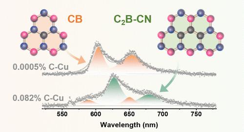
Visible-range single-photon emitters (SPEs), based on hexagonal boron nitride (hBN), with exceptional optical performance have become an outstanding candidate for quantum optical technology. However, the control of the carbon defect structures to obtain uniform and confined band structure remains elusive, restricting their integration into on-chip quantum devices. Here, we demonstrate tuning of the defect structure of hBN to precisely control the emission in SPEs. The defect structure engineering from CB (carbon substituted at the boron site) to C2B–CN (carbon doped into two boron sites and one nitrogen site) carbon defect conversion in hBN is realized by regulating the carbon concentration from 0.0005 at % to 0.082 at % in Cu substrates to adjust the carbon diffusion during the CVD process. Meanwhile, the zero-phonon line exhibits a precise shift from the range of 600–610 nm to 630–640 nm; these shifts of the spectral features are further supported by density functional theory results, reflected in changes in the band structure, vibrational degrees of freedom, and electronic transitions. The SPE emission spectrum serves as a valuable tool for identifying the footprint of a carbon point defect structure change. Our project offers evidence of achieving structured defect engineering for tailored emission properties and showcases potential for the integration of advanced 2D material engineering into on-chip quantum devices.
期刊介绍:
ACS Nano, published monthly, serves as an international forum for comprehensive articles on nanoscience and nanotechnology research at the intersections of chemistry, biology, materials science, physics, and engineering. The journal fosters communication among scientists in these communities, facilitating collaboration, new research opportunities, and advancements through discoveries. ACS Nano covers synthesis, assembly, characterization, theory, and simulation of nanostructures, nanobiotechnology, nanofabrication, methods and tools for nanoscience and nanotechnology, and self- and directed-assembly. Alongside original research articles, it offers thorough reviews, perspectives on cutting-edge research, and discussions envisioning the future of nanoscience and nanotechnology.


 分享
分享
 求助内容:
求助内容: 应助结果提醒方式:
 扫码关注我们
