Ragib Ahsan, Anika Tabassum Priyoti, Jun Meng, Ryan Jacobs, John Booske, Rehan Kapadia
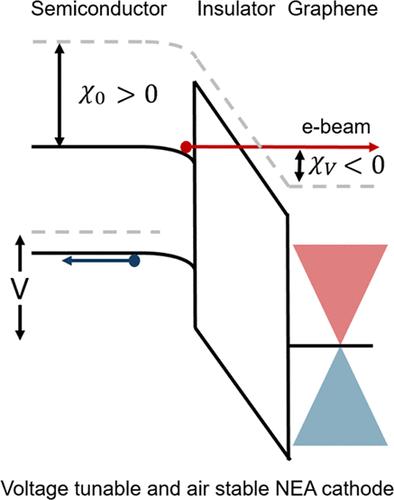
{"title":"Hot Electron Photoemission from Tunable Electron Affinity Semiconductor Cathodes","authors":"Ragib Ahsan, Anika Tabassum Priyoti, Jun Meng, Ryan Jacobs, John Booske, Rehan Kapadia","doi":"10.1021/acsami.4c18187","DOIUrl":null,"url":null,"abstract":"A voltage-tunable negative electron affinity (NEA) semiconductor photocathode offers one key advantage over current materials such as cesiated NEA photocathodes: stability under ambient conditions. A semiconductor/insulator/graphene heterostructure can inject electrons into the conduction band of the insulator, where an electric field “heats” them up so that the effective emission barrier seen by the “hot” electrons is negative, enabling a voltage-tunable NEA surface. Here, we have experimentally demonstrated a peak emission current density of 2.253 × 10<sup>–3</sup> A/cm<sup>2</sup> and a peak external quantum efficiency (EQE) of ∼1.53% from a p-Si/amorphous-Al<sub>2</sub>O<sub>3</sub>/graphene-based hot electron laser-assisted cathode (HELAC). We have developed a full-band Monte Carlo Boltzmann Transport Equation (MCBTE) solver to study the hot electron transport behavior in three different crystalline insulators: SiO<sub>2</sub>, Al<sub>2</sub>O<sub>3</sub>, and MgO. Through MCBTE and semiconductor device simulations, we have predicted a peak emission current density of ∼10<sup>3</sup> A/cm<sup>2</sup>, far above our experimental value, indicating that the optimal performance of state-of-the-art HELACs has not yet been realized. This theoretical framework provides an understanding of the key performance limitations of the device and can be used to guide the optimal design (e.g., through the selection of new materials) of voltage-tunable NEA semiconductor photocathodes.","PeriodicalId":5,"journal":{"name":"ACS Applied Materials & Interfaces","volume":"16 1","pages":""},"PeriodicalIF":8.3000,"publicationDate":"2025-03-06","publicationTypes":"Journal Article","fieldsOfStudy":null,"isOpenAccess":false,"openAccessPdf":"","citationCount":"0","resultStr":null,"platform":"Semanticscholar","paperid":null,"PeriodicalName":"ACS Applied Materials & Interfaces","FirstCategoryId":"88","ListUrlMain":"https://doi.org/10.1021/acsami.4c18187","RegionNum":2,"RegionCategory":"材料科学","ArticlePicture":[],"TitleCN":null,"AbstractTextCN":null,"PMCID":null,"EPubDate":"","PubModel":"","JCR":"Q1","JCRName":"MATERIALS SCIENCE, MULTIDISCIPLINARY","Score":null,"Total":0}
引用次数: 0
Abstract
A voltage-tunable negative electron affinity (NEA) semiconductor photocathode offers one key advantage over current materials such as cesiated NEA photocathodes: stability under ambient conditions. A semiconductor/insulator/graphene heterostructure can inject electrons into the conduction band of the insulator, where an electric field “heats” them up so that the effective emission barrier seen by the “hot” electrons is negative, enabling a voltage-tunable NEA surface. Here, we have experimentally demonstrated a peak emission current density of 2.253 × 10⁻³ A/cm2 and a peak external quantum efficiency (EQE) of ∼1.53% from a p-Si/amorphous-Al2O3/graphene-based hot electron laser-assisted cathode (HELAC). We have developed a full-band Monte Carlo Boltzmann Transport Equation (MCBTE) solver to study the hot electron transport behavior in three different crystalline insulators: SiO2, Al2O3, and MgO. Through MCBTE and semiconductor device simulations, we have predicted a peak emission current density of ∼103 A/cm2, far above our experimental value, indicating that the optimal performance of state-of-the-art HELACs has not yet been realized. This theoretical framework provides an understanding of the key performance limitations of the device and can be used to guide the optimal design (e.g., through the selection of new materials) of voltage-tunable NEA semiconductor photocathodes.
期刊介绍:
ACS Applied Materials & Interfaces is a leading interdisciplinary journal that brings together chemists, engineers, physicists, and biologists to explore the development and utilization of newly-discovered materials and interfacial processes for specific applications. Our journal has experienced remarkable growth since its establishment in 2009, both in terms of the number of articles published and the impact of the research showcased. We are proud to foster a truly global community, with the majority of published articles originating from outside the United States, reflecting the rapid growth of applied research worldwide.


 分享
分享
 求助内容:
求助内容: 应助结果提醒方式:
 扫码关注我们
