{"title":"模拟基于未掺杂 AlxGa1-xAs 量子纳米线的垂直弹道量子势垒场效应晶体管","authors":"D. V. Pozdnyakov, A. V. Borzdov, V. M. Borzdov","doi":"10.1134/s1063739723700749","DOIUrl":null,"url":null,"abstract":"<h3 data-test=\"abstract-sub-heading\">Abstract</h3><p>A design and topological solution for a tunnel field-effect transistor of a new type is proposed and the simulation of the transistor is performed. The device is a vertical ballistic field-effect transistor with a cylindrical metallic gate based on a cylindrical undoped Al<sub><i>x</i></sub>Ga<sub>1–<i>x</i></sub>As quantum nanowire located in an Al<sub>2</sub>O<sub>3</sub> matrix. For the given geometry of the device structure, the optimum of the fraction of aluminum in the semiconductor composition varying along the transistor channel is found, at which, unlike a conventional tunnel field-effect transistor, not only is the complete suppression of the quantum barrier for electrons by a positive gate voltage ensured but also the minimum possible electrical resistance of the transistor channel is achieved. The current-voltage characteristics of the transistor are calculated within the framework of a rigorous quantum-mechanical description of the electron transport in its channel, taking into account the nonparabolic nature of the band structure of the semiconductor.</p>","PeriodicalId":21534,"journal":{"name":"Russian Microelectronics","volume":"5 1","pages":""},"PeriodicalIF":0.0000,"publicationDate":"2024-02-08","publicationTypes":"Journal Article","fieldsOfStudy":null,"isOpenAccess":false,"openAccessPdf":"","citationCount":"0","resultStr":"{\"title\":\"Simulation of a Vertical Ballistic Quantum-Barrier Field-Effect Transistor Based on an Undoped AlxGa1–xAs Quantum Nanowire\",\"authors\":\"D. V. Pozdnyakov, A. V. Borzdov, V. M. Borzdov\",\"doi\":\"10.1134/s1063739723700749\",\"DOIUrl\":null,\"url\":null,\"abstract\":\"<h3 data-test=\\\"abstract-sub-heading\\\">Abstract</h3><p>A design and topological solution for a tunnel field-effect transistor of a new type is proposed and the simulation of the transistor is performed. The device is a vertical ballistic field-effect transistor with a cylindrical metallic gate based on a cylindrical undoped Al<sub><i>x</i></sub>Ga<sub>1–<i>x</i></sub>As quantum nanowire located in an Al<sub>2</sub>O<sub>3</sub> matrix. For the given geometry of the device structure, the optimum of the fraction of aluminum in the semiconductor composition varying along the transistor channel is found, at which, unlike a conventional tunnel field-effect transistor, not only is the complete suppression of the quantum barrier for electrons by a positive gate voltage ensured but also the minimum possible electrical resistance of the transistor channel is achieved. The current-voltage characteristics of the transistor are calculated within the framework of a rigorous quantum-mechanical description of the electron transport in its channel, taking into account the nonparabolic nature of the band structure of the semiconductor.</p>\",\"PeriodicalId\":21534,\"journal\":{\"name\":\"Russian Microelectronics\",\"volume\":\"5 1\",\"pages\":\"\"},\"PeriodicalIF\":0.0000,\"publicationDate\":\"2024-02-08\",\"publicationTypes\":\"Journal Article\",\"fieldsOfStudy\":null,\"isOpenAccess\":false,\"openAccessPdf\":\"\",\"citationCount\":\"0\",\"resultStr\":null,\"platform\":\"Semanticscholar\",\"paperid\":null,\"PeriodicalName\":\"Russian Microelectronics\",\"FirstCategoryId\":\"1085\",\"ListUrlMain\":\"https://doi.org/10.1134/s1063739723700749\",\"RegionNum\":0,\"RegionCategory\":null,\"ArticlePicture\":[],\"TitleCN\":null,\"AbstractTextCN\":null,\"PMCID\":null,\"EPubDate\":\"\",\"PubModel\":\"\",\"JCR\":\"Q4\",\"JCRName\":\"Engineering\",\"Score\":null,\"Total\":0}","platform":"Semanticscholar","paperid":null,"PeriodicalName":"Russian Microelectronics","FirstCategoryId":"1085","ListUrlMain":"https://doi.org/10.1134/s1063739723700749","RegionNum":0,"RegionCategory":null,"ArticlePicture":[],"TitleCN":null,"AbstractTextCN":null,"PMCID":null,"EPubDate":"","PubModel":"","JCR":"Q4","JCRName":"Engineering","Score":null,"Total":0}
Simulation of a Vertical Ballistic Quantum-Barrier Field-Effect Transistor Based on an Undoped AlxGa1–xAs Quantum Nanowire
Abstract
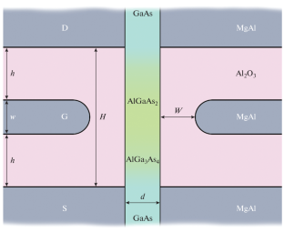
A design and topological solution for a tunnel field-effect transistor of a new type is proposed and the simulation of the transistor is performed. The device is a vertical ballistic field-effect transistor with a cylindrical metallic gate based on a cylindrical undoped AlxGa1–xAs quantum nanowire located in an Al2O3 matrix. For the given geometry of the device structure, the optimum of the fraction of aluminum in the semiconductor composition varying along the transistor channel is found, at which, unlike a conventional tunnel field-effect transistor, not only is the complete suppression of the quantum barrier for electrons by a positive gate voltage ensured but also the minimum possible electrical resistance of the transistor channel is achieved. The current-voltage characteristics of the transistor are calculated within the framework of a rigorous quantum-mechanical description of the electron transport in its channel, taking into account the nonparabolic nature of the band structure of the semiconductor.
期刊介绍:
Russian Microelectronics covers physical, technological, and some VLSI and ULSI circuit-technical aspects of microelectronics and nanoelectronics; it informs the reader of new trends in submicron optical, x-ray, electron, and ion-beam lithography technology; dry processing techniques, etching, doping; and deposition and planarization technology. Significant space is devoted to problems arising in the application of proton, electron, and ion beams, plasma, etc. Consideration is given to new equipment, including cluster tools and control in situ and submicron CMOS, bipolar, and BICMOS technologies. The journal publishes papers addressing problems of molecular beam epitaxy and related processes; heterojunction devices and integrated circuits; the technology and devices of nanoelectronics; and the fabrication of nanometer scale devices, including new device structures, quantum-effect devices, and superconducting devices. The reader will find papers containing news of the diagnostics of surfaces and microelectronic structures, the modeling of technological processes and devices in micro- and nanoelectronics, including nanotransistors, and solid state qubits.


 分享
分享
 求助内容:
求助内容: 应助结果提醒方式:
 扫码关注我们
