R. Aliasgari Renani, O. A. Soltanovich, M. A. Knyazev, S. V. Koveshnikov
{"title":"通过电容-电压和热激励电流技术研究低能电子辐照二氧化硅基 MOS 器件","authors":"R. Aliasgari Renani, O. A. Soltanovich, M. A. Knyazev, S. V. Koveshnikov","doi":"10.1134/s1063739723600516","DOIUrl":null,"url":null,"abstract":"<h3 data-test=\"abstract-sub-heading\">Abstract</h3><p>Silicon oxide based and aluminum gated MOS structures fabricated on n-type silicon are investigated after irradiation with low energy electrons in scanning electron microscope. The thermally stimulated current (TSC) technique in the temperature range from 80 K to 320 K revealed a number of the electron beam induced charge traps. With the help of the capacitance-voltage method, the traps revealed by the TSC were identified by their location (within dielectric, semiconductor or at the interface) and by their nature (trap for electrons or for holes).</p>","PeriodicalId":21534,"journal":{"name":"Russian Microelectronics","volume":"16 1","pages":""},"PeriodicalIF":0.0000,"publicationDate":"2024-03-21","publicationTypes":"Journal Article","fieldsOfStudy":null,"isOpenAccess":false,"openAccessPdf":"","citationCount":"0","resultStr":"{\"title\":\"Investigation of Low Energy Electron Irradiated SiO2 Based MOS Devices by Capacitance-Voltage and Thermally Stimulated Current Techniques\",\"authors\":\"R. Aliasgari Renani, O. A. Soltanovich, M. A. Knyazev, S. V. Koveshnikov\",\"doi\":\"10.1134/s1063739723600516\",\"DOIUrl\":null,\"url\":null,\"abstract\":\"<h3 data-test=\\\"abstract-sub-heading\\\">Abstract</h3><p>Silicon oxide based and aluminum gated MOS structures fabricated on n-type silicon are investigated after irradiation with low energy electrons in scanning electron microscope. The thermally stimulated current (TSC) technique in the temperature range from 80 K to 320 K revealed a number of the electron beam induced charge traps. With the help of the capacitance-voltage method, the traps revealed by the TSC were identified by their location (within dielectric, semiconductor or at the interface) and by their nature (trap for electrons or for holes).</p>\",\"PeriodicalId\":21534,\"journal\":{\"name\":\"Russian Microelectronics\",\"volume\":\"16 1\",\"pages\":\"\"},\"PeriodicalIF\":0.0000,\"publicationDate\":\"2024-03-21\",\"publicationTypes\":\"Journal Article\",\"fieldsOfStudy\":null,\"isOpenAccess\":false,\"openAccessPdf\":\"\",\"citationCount\":\"0\",\"resultStr\":null,\"platform\":\"Semanticscholar\",\"paperid\":null,\"PeriodicalName\":\"Russian Microelectronics\",\"FirstCategoryId\":\"1085\",\"ListUrlMain\":\"https://doi.org/10.1134/s1063739723600516\",\"RegionNum\":0,\"RegionCategory\":null,\"ArticlePicture\":[],\"TitleCN\":null,\"AbstractTextCN\":null,\"PMCID\":null,\"EPubDate\":\"\",\"PubModel\":\"\",\"JCR\":\"Q4\",\"JCRName\":\"Engineering\",\"Score\":null,\"Total\":0}","platform":"Semanticscholar","paperid":null,"PeriodicalName":"Russian Microelectronics","FirstCategoryId":"1085","ListUrlMain":"https://doi.org/10.1134/s1063739723600516","RegionNum":0,"RegionCategory":null,"ArticlePicture":[],"TitleCN":null,"AbstractTextCN":null,"PMCID":null,"EPubDate":"","PubModel":"","JCR":"Q4","JCRName":"Engineering","Score":null,"Total":0}
引用次数: 0
摘要
摘要 在扫描电子显微镜下,研究了用低能量电子辐照在 n 型硅上制作的氧化硅基和铝栅 MOS 结构。热激励电流(TSC)技术在 80 K 至 320 K 的温度范围内揭示了一些电子束诱导的电荷陷阱。在电容-电压法的帮助下,通过位置(介质、半导体或界面)和性质(电子或空穴陷阱)确定了热刺激电流技术所揭示的陷阱。
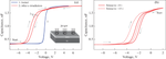
Investigation of Low Energy Electron Irradiated SiO2 Based MOS Devices by Capacitance-Voltage and Thermally Stimulated Current Techniques
Abstract
Silicon oxide based and aluminum gated MOS structures fabricated on n-type silicon are investigated after irradiation with low energy electrons in scanning electron microscope. The thermally stimulated current (TSC) technique in the temperature range from 80 K to 320 K revealed a number of the electron beam induced charge traps. With the help of the capacitance-voltage method, the traps revealed by the TSC were identified by their location (within dielectric, semiconductor or at the interface) and by their nature (trap for electrons or for holes).
期刊介绍:
Russian Microelectronics covers physical, technological, and some VLSI and ULSI circuit-technical aspects of microelectronics and nanoelectronics; it informs the reader of new trends in submicron optical, x-ray, electron, and ion-beam lithography technology; dry processing techniques, etching, doping; and deposition and planarization technology. Significant space is devoted to problems arising in the application of proton, electron, and ion beams, plasma, etc. Consideration is given to new equipment, including cluster tools and control in situ and submicron CMOS, bipolar, and BICMOS technologies. The journal publishes papers addressing problems of molecular beam epitaxy and related processes; heterojunction devices and integrated circuits; the technology and devices of nanoelectronics; and the fabrication of nanometer scale devices, including new device structures, quantum-effect devices, and superconducting devices. The reader will find papers containing news of the diagnostics of surfaces and microelectronic structures, the modeling of technological processes and devices in micro- and nanoelectronics, including nanotransistors, and solid state qubits.


 分享
分享
 求助内容:
求助内容: 应助结果提醒方式:
 扫码关注我们
