Amit Kumar Verma, Rachana Gupta, Shashi Prakash, Andrei Gloskovskii, Shailesh Kalal, Priyanshi Tiwari, Varimalla Raghavendra Reddy, Rajeev Rawat, Mukul Gupta
{"title":"外延和多晶钒钛薄膜的结构与超导性","authors":"Amit Kumar Verma, Rachana Gupta, Shashi Prakash, Andrei Gloskovskii, Shailesh Kalal, Priyanshi Tiwari, Varimalla Raghavendra Reddy, Rajeev Rawat, Mukul Gupta","doi":"10.1021/acsaelm.4c00540","DOIUrl":null,"url":null,"abstract":"In this work, we present a systematic study of superconducting vanadium mononitride (VN) thin films that were simultaneously grown on single crystalline MgO (100) and amorphous SiO<sub>2</sub> substrates. The structure of both samples was probed using X-ray diffraction measurements under different geometries, i.e., specular, off-specular, and ϕ-scan. It was found that the lattice parameter (LP) of VN films grown on SiO<sub>2</sub> was 4.098(7) Å, while on MgO, it was slightly larger at 4.124(2) Å. Though the LP of both samples is within the experimentally obtained and theoretically predicted values, the obtained difference suggests that the polycrystalline VN has a tensile strain as compared to the epitaxial film. The effect of such strain is more clearly reflected on the superconducting transition temperature (<i>T</i><sub>C</sub>) and normal state electrical resistivity (ρ<sub><i>n</i></sub>). In case of the epitaxial VN sample, the <i>T</i><sub>C</sub> was at 8.1 K, while in the polycrystalline sample, it was at 5.2 K. The ρ<sub><i>n</i></sub> was also found to be significantly smaller in epitaxial films, suggesting a better crystalline quality. We performed X-ray absorption and hard X-ray photoelectron spectroscopy measurements to probe the electronic structure. It was found that the surface region of polycrystalline or epitaxial samples remains unaffected by such strains. However, high magnetic field resistivity measurements exhibited a two-step <i>T</i><sub>C</sub> in the epitaxial film which originates due to formation of a thin strained region formed during the initial stages of growth. Our in situ reflection high energy electron diffraction measurements confirmed that the initial stages of growth is strained due to lattice mismatch of about +2.13% between MgO and VN. Overall, this comparative study of epitaxial and polycrystalline samples elucidates the role of stress and strain on the structural, electronic, and superconducting properties of VN thin films.","PeriodicalId":3,"journal":{"name":"ACS Applied Electronic Materials","volume":null,"pages":null},"PeriodicalIF":4.3000,"publicationDate":"2024-06-25","publicationTypes":"Journal Article","fieldsOfStudy":null,"isOpenAccess":false,"openAccessPdf":"","citationCount":"0","resultStr":"{\"title\":\"Structure and Superconductivity of Epitaxial and Polycrystalline VN Thin Films\",\"authors\":\"Amit Kumar Verma, Rachana Gupta, Shashi Prakash, Andrei Gloskovskii, Shailesh Kalal, Priyanshi Tiwari, Varimalla Raghavendra Reddy, Rajeev Rawat, Mukul Gupta\",\"doi\":\"10.1021/acsaelm.4c00540\",\"DOIUrl\":null,\"url\":null,\"abstract\":\"In this work, we present a systematic study of superconducting vanadium mononitride (VN) thin films that were simultaneously grown on single crystalline MgO (100) and amorphous SiO<sub>2</sub> substrates. The structure of both samples was probed using X-ray diffraction measurements under different geometries, i.e., specular, off-specular, and ϕ-scan. It was found that the lattice parameter (LP) of VN films grown on SiO<sub>2</sub> was 4.098(7) Å, while on MgO, it was slightly larger at 4.124(2) Å. Though the LP of both samples is within the experimentally obtained and theoretically predicted values, the obtained difference suggests that the polycrystalline VN has a tensile strain as compared to the epitaxial film. The effect of such strain is more clearly reflected on the superconducting transition temperature (<i>T</i><sub>C</sub>) and normal state electrical resistivity (ρ<sub><i>n</i></sub>). In case of the epitaxial VN sample, the <i>T</i><sub>C</sub> was at 8.1 K, while in the polycrystalline sample, it was at 5.2 K. The ρ<sub><i>n</i></sub> was also found to be significantly smaller in epitaxial films, suggesting a better crystalline quality. We performed X-ray absorption and hard X-ray photoelectron spectroscopy measurements to probe the electronic structure. It was found that the surface region of polycrystalline or epitaxial samples remains unaffected by such strains. However, high magnetic field resistivity measurements exhibited a two-step <i>T</i><sub>C</sub> in the epitaxial film which originates due to formation of a thin strained region formed during the initial stages of growth. Our in situ reflection high energy electron diffraction measurements confirmed that the initial stages of growth is strained due to lattice mismatch of about +2.13% between MgO and VN. Overall, this comparative study of epitaxial and polycrystalline samples elucidates the role of stress and strain on the structural, electronic, and superconducting properties of VN thin films.\",\"PeriodicalId\":3,\"journal\":{\"name\":\"ACS Applied Electronic Materials\",\"volume\":null,\"pages\":null},\"PeriodicalIF\":4.3000,\"publicationDate\":\"2024-06-25\",\"publicationTypes\":\"Journal Article\",\"fieldsOfStudy\":null,\"isOpenAccess\":false,\"openAccessPdf\":\"\",\"citationCount\":\"0\",\"resultStr\":null,\"platform\":\"Semanticscholar\",\"paperid\":null,\"PeriodicalName\":\"ACS Applied Electronic Materials\",\"FirstCategoryId\":\"88\",\"ListUrlMain\":\"https://doi.org/10.1021/acsaelm.4c00540\",\"RegionNum\":3,\"RegionCategory\":\"材料科学\",\"ArticlePicture\":[],\"TitleCN\":null,\"AbstractTextCN\":null,\"PMCID\":null,\"EPubDate\":\"\",\"PubModel\":\"\",\"JCR\":\"Q1\",\"JCRName\":\"ENGINEERING, ELECTRICAL & ELECTRONIC\",\"Score\":null,\"Total\":0}","platform":"Semanticscholar","paperid":null,"PeriodicalName":"ACS Applied Electronic Materials","FirstCategoryId":"88","ListUrlMain":"https://doi.org/10.1021/acsaelm.4c00540","RegionNum":3,"RegionCategory":"材料科学","ArticlePicture":[],"TitleCN":null,"AbstractTextCN":null,"PMCID":null,"EPubDate":"","PubModel":"","JCR":"Q1","JCRName":"ENGINEERING, ELECTRICAL & ELECTRONIC","Score":null,"Total":0}
引用次数: 0
摘要
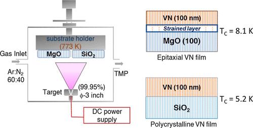
在这项工作中,我们对同时生长在单晶氧化镁(100)和无定形二氧化硅基底上的超导单氮化钒(VN)薄膜进行了系统研究。在不同的几何条件下,即镜面、非镜面和ϕ扫描条件下,使用 X 射线衍射测量探究了这两种样品的结构。结果发现,在二氧化硅上生长的 VN 薄膜的晶格参数(LP)为 4.098(7) Å,而在氧化镁上生长的 VN 薄膜的晶格参数(LP)稍大,为 4.124(2) Å。这种应变对超导转变温度(TC)和正常状态电阻率(ρn)的影响更为明显。外延 VN 样品的超导转变温度为 8.1 K,而多晶样品的超导转变温度为 5.2 K。我们进行了 X 射线吸收和硬 X 射线光电子能谱测量,以探测电子结构。结果发现,多晶或外延样品的表面区域不受这种应变的影响。然而,高磁场电阻率测量显示,外延薄膜中存在两级 TC,这是由于在生长的初始阶段形成了一个薄的应变区域。我们的原位反射高能电子衍射测量结果证实,生长的初始阶段由于氧化镁和 VN 之间约 +2.13% 的晶格失配而产生应变。总之,这项关于外延和多晶样品的比较研究阐明了应力和应变对 VN 薄膜的结构、电子和超导特性的影响。
Structure and Superconductivity of Epitaxial and Polycrystalline VN Thin Films
In this work, we present a systematic study of superconducting vanadium mononitride (VN) thin films that were simultaneously grown on single crystalline MgO (100) and amorphous SiO2 substrates. The structure of both samples was probed using X-ray diffraction measurements under different geometries, i.e., specular, off-specular, and ϕ-scan. It was found that the lattice parameter (LP) of VN films grown on SiO2 was 4.098(7) Å, while on MgO, it was slightly larger at 4.124(2) Å. Though the LP of both samples is within the experimentally obtained and theoretically predicted values, the obtained difference suggests that the polycrystalline VN has a tensile strain as compared to the epitaxial film. The effect of such strain is more clearly reflected on the superconducting transition temperature (TC) and normal state electrical resistivity (ρn). In case of the epitaxial VN sample, the TC was at 8.1 K, while in the polycrystalline sample, it was at 5.2 K. The ρn was also found to be significantly smaller in epitaxial films, suggesting a better crystalline quality. We performed X-ray absorption and hard X-ray photoelectron spectroscopy measurements to probe the electronic structure. It was found that the surface region of polycrystalline or epitaxial samples remains unaffected by such strains. However, high magnetic field resistivity measurements exhibited a two-step TC in the epitaxial film which originates due to formation of a thin strained region formed during the initial stages of growth. Our in situ reflection high energy electron diffraction measurements confirmed that the initial stages of growth is strained due to lattice mismatch of about +2.13% between MgO and VN. Overall, this comparative study of epitaxial and polycrystalline samples elucidates the role of stress and strain on the structural, electronic, and superconducting properties of VN thin films.


 分享
分享
 求助内容:
求助内容: 应助结果提醒方式:
 扫码关注我们
