{"title":"集成驱动器和功率 HEMT 的氮化镓半桥集成电路的热建模和布局优化","authors":"V. A. Kagadey, I. Y. Kodorova, E. S. Polyntsev","doi":"10.1134/s1063739724600225","DOIUrl":null,"url":null,"abstract":"<h3 data-test=\"abstract-sub-heading\">Abstract</h3><p>The paper presents the results of thermal modeling of a half-bridge monolithic integrated circuit (IC) with integrated drivers and enhanced mode power high electron mobility transistors, based on a GaN-on-SOI heterostructure. It had been established that the main heat sources in the IC were the half-bridge GaN HEMTs. The heat from the half-bridge GaN HEMTs propagates in the chip and leads to heating of the logic block and gate drivers. Heating of half-bridge GaN HEMTs leads to increased channel resistance and IC output current drop. Heating of the gate drivers reduces driving current, as a result, increases the switching time of the half-bridge GaN HEMTs. Heating of the logic block increases the rise and fall times of the generated control signals, which worsens the dynamic characteristics of the IC. A comparative analysis of heat propagation for IC dies based on GaN-on-SOI and GaN-on-Si heterostructures showed that GaN-on-SOI structure has a 40% greater junction-to-backside thermal resistivity compared to GaN-on-Si structure. In this case, the specific thermal resistance in the direction of heat propagation from the hotspot of the transistor to the backside of the die for the GaN-on-SOI structure is almost two orders of magnitude greater than in the direction of its propagation to the frontside of the chip. The results obtained were used for IC layout optimization. The rearrangement of GaN-on-SOI IC functional blocks, as well as to introduction of additional heat-spreading elements on the frontside of chip were carried out during the optimization.</p>","PeriodicalId":21534,"journal":{"name":"Russian Microelectronics","volume":"69 1","pages":""},"PeriodicalIF":0.0000,"publicationDate":"2024-07-26","publicationTypes":"Journal Article","fieldsOfStudy":null,"isOpenAccess":false,"openAccessPdf":"","citationCount":"0","resultStr":"{\"title\":\"Thermal Modeling and Layout Optimization of GaN Half-Bridge IC with Integrated Drivers and Power HEMTs\",\"authors\":\"V. A. Kagadey, I. Y. Kodorova, E. S. Polyntsev\",\"doi\":\"10.1134/s1063739724600225\",\"DOIUrl\":null,\"url\":null,\"abstract\":\"<h3 data-test=\\\"abstract-sub-heading\\\">Abstract</h3><p>The paper presents the results of thermal modeling of a half-bridge monolithic integrated circuit (IC) with integrated drivers and enhanced mode power high electron mobility transistors, based on a GaN-on-SOI heterostructure. It had been established that the main heat sources in the IC were the half-bridge GaN HEMTs. The heat from the half-bridge GaN HEMTs propagates in the chip and leads to heating of the logic block and gate drivers. Heating of half-bridge GaN HEMTs leads to increased channel resistance and IC output current drop. Heating of the gate drivers reduces driving current, as a result, increases the switching time of the half-bridge GaN HEMTs. Heating of the logic block increases the rise and fall times of the generated control signals, which worsens the dynamic characteristics of the IC. A comparative analysis of heat propagation for IC dies based on GaN-on-SOI and GaN-on-Si heterostructures showed that GaN-on-SOI structure has a 40% greater junction-to-backside thermal resistivity compared to GaN-on-Si structure. In this case, the specific thermal resistance in the direction of heat propagation from the hotspot of the transistor to the backside of the die for the GaN-on-SOI structure is almost two orders of magnitude greater than in the direction of its propagation to the frontside of the chip. The results obtained were used for IC layout optimization. The rearrangement of GaN-on-SOI IC functional blocks, as well as to introduction of additional heat-spreading elements on the frontside of chip were carried out during the optimization.</p>\",\"PeriodicalId\":21534,\"journal\":{\"name\":\"Russian Microelectronics\",\"volume\":\"69 1\",\"pages\":\"\"},\"PeriodicalIF\":0.0000,\"publicationDate\":\"2024-07-26\",\"publicationTypes\":\"Journal Article\",\"fieldsOfStudy\":null,\"isOpenAccess\":false,\"openAccessPdf\":\"\",\"citationCount\":\"0\",\"resultStr\":null,\"platform\":\"Semanticscholar\",\"paperid\":null,\"PeriodicalName\":\"Russian Microelectronics\",\"FirstCategoryId\":\"1085\",\"ListUrlMain\":\"https://doi.org/10.1134/s1063739724600225\",\"RegionNum\":0,\"RegionCategory\":null,\"ArticlePicture\":[],\"TitleCN\":null,\"AbstractTextCN\":null,\"PMCID\":null,\"EPubDate\":\"\",\"PubModel\":\"\",\"JCR\":\"Q4\",\"JCRName\":\"Engineering\",\"Score\":null,\"Total\":0}","platform":"Semanticscholar","paperid":null,"PeriodicalName":"Russian Microelectronics","FirstCategoryId":"1085","ListUrlMain":"https://doi.org/10.1134/s1063739724600225","RegionNum":0,"RegionCategory":null,"ArticlePicture":[],"TitleCN":null,"AbstractTextCN":null,"PMCID":null,"EPubDate":"","PubModel":"","JCR":"Q4","JCRName":"Engineering","Score":null,"Total":0}
引用次数: 0
摘要
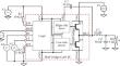
摘要 本文介绍了基于 GaN-on-SOI 异质结构、集成了驱动器和增强型功率高电子迁移率晶体管的半桥单片集成电路(IC)的热建模结果。已确定集成电路中的主要热源是半桥 GaN HEMT。来自半桥 GaN HEMT 的热量在芯片中传播,导致逻辑块和栅极驱动器发热。半桥氮化镓 HEMT 的发热会导致通道电阻增加和集成电路输出电流下降。栅极驱动器发热会降低驱动电流,从而延长半桥 GaN HEMT 的开关时间。逻辑块发热会增加生成的控制信号的上升和下降时间,从而使集成电路的动态特性恶化。对基于硅基氮化镓和硅基氮化镓异质结构的集成电路芯片进行的热传播比较分析表明,硅基氮化镓结构的结至背面热阻比硅基氮化镓结构高 40%。在这种情况下,GaN-on-SOI 结构从晶体管热点到芯片背面的热传播方向上的比热阻几乎比向芯片正面传播方向上的比热阻大两个数量级。所得结果用于集成电路布局优化。在优化过程中,对硅基氮化镓集成电路功能块进行了重新排列,并在芯片正面引入了额外的散热元件。
Thermal Modeling and Layout Optimization of GaN Half-Bridge IC with Integrated Drivers and Power HEMTs
Abstract
The paper presents the results of thermal modeling of a half-bridge monolithic integrated circuit (IC) with integrated drivers and enhanced mode power high electron mobility transistors, based on a GaN-on-SOI heterostructure. It had been established that the main heat sources in the IC were the half-bridge GaN HEMTs. The heat from the half-bridge GaN HEMTs propagates in the chip and leads to heating of the logic block and gate drivers. Heating of half-bridge GaN HEMTs leads to increased channel resistance and IC output current drop. Heating of the gate drivers reduces driving current, as a result, increases the switching time of the half-bridge GaN HEMTs. Heating of the logic block increases the rise and fall times of the generated control signals, which worsens the dynamic characteristics of the IC. A comparative analysis of heat propagation for IC dies based on GaN-on-SOI and GaN-on-Si heterostructures showed that GaN-on-SOI structure has a 40% greater junction-to-backside thermal resistivity compared to GaN-on-Si structure. In this case, the specific thermal resistance in the direction of heat propagation from the hotspot of the transistor to the backside of the die for the GaN-on-SOI structure is almost two orders of magnitude greater than in the direction of its propagation to the frontside of the chip. The results obtained were used for IC layout optimization. The rearrangement of GaN-on-SOI IC functional blocks, as well as to introduction of additional heat-spreading elements on the frontside of chip were carried out during the optimization.
期刊介绍:
Russian Microelectronics covers physical, technological, and some VLSI and ULSI circuit-technical aspects of microelectronics and nanoelectronics; it informs the reader of new trends in submicron optical, x-ray, electron, and ion-beam lithography technology; dry processing techniques, etching, doping; and deposition and planarization technology. Significant space is devoted to problems arising in the application of proton, electron, and ion beams, plasma, etc. Consideration is given to new equipment, including cluster tools and control in situ and submicron CMOS, bipolar, and BICMOS technologies. The journal publishes papers addressing problems of molecular beam epitaxy and related processes; heterojunction devices and integrated circuits; the technology and devices of nanoelectronics; and the fabrication of nanometer scale devices, including new device structures, quantum-effect devices, and superconducting devices. The reader will find papers containing news of the diagnostics of surfaces and microelectronic structures, the modeling of technological processes and devices in micro- and nanoelectronics, including nanotransistors, and solid state qubits.


 分享
分享
 求助内容:
求助内容: 应助结果提醒方式:
 扫码关注我们
